High-Speed Signal PCB Routing,transmission line theory is essential. Some methods differ from traditional signal routing. Here are some key high speed signal routing techniques:
Impedance Continuity Control
Discontinuities Caused by Line Width Changes
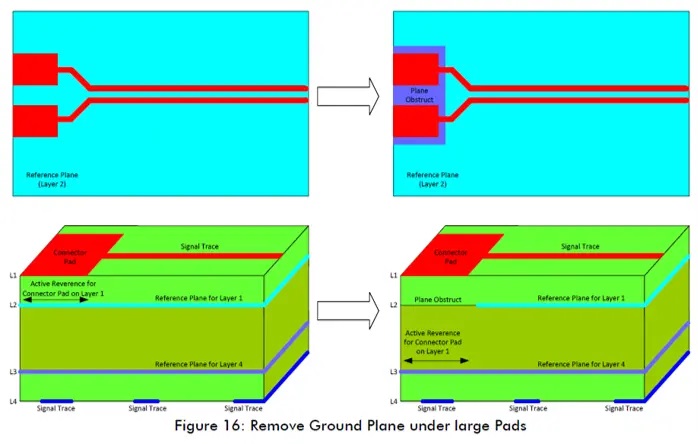
The impedance of a trace typically depends on its width and the distance to the reference plane. Wider traces have lower impedance. In cases where a large pad is connected to a narrow high-speed trace, the pad’s impedance is lower, but the trace’s impedance is higher, leading to impedance mismatch and signal reflections. To resolve this, a copper pour should be placed beneath the pad, with a reference plane on another layer to increase impedance and ensure continuity.

Discontinuities Caused by Vias
Vias can also cause impedance mismatch. To minimize this effect, unwanted copper on the inner layers connected to vias should be removed. This can be done during design using CAD tools or by coordinating with the PCB manufacturer to eliminate unnecessary copper and ensure impedance continuity.

High-Speed Differential Signal Design
Symmetry Requirements
For high-speed differential signals, the traces must have equal width and spacing to achieve the desired differential impedance. Therefore, ensure symmetry when routing differential signal pairs. When coupling capacitors are used, they should also be symmetrically placed, and capacitors should be small, preferably 0402 or 0603 packages—avoid using larger capacitors like 0805 or parallel capacitors.

Discontinuities Caused by Components and Vias
Do not place vias or components within the differential pair. Doing so can cause EMC issues and impedance discontinuities. Vias introduce significant impedance mismatches, so minimize their use in differential pairs, and if necessary, place them symmetrically.

Length Matching Requirements
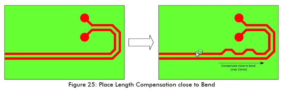
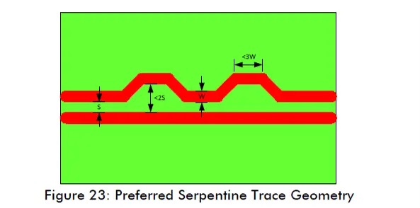
For high-speed signal PCB interfaces, such as buses, the signal arrival time and skew between traces must be minimized to maintain synchronization. This can be achieved by length matching the signal traces, which ensures that the timing of the signals remains consistent. In high-speed differential pairs, the two traces must also have matched delay, or communication may fail. To achieve this, serpentine routing can be used at the source to compensate for length mismatches.

Bends in traces are a common source of length mismatch, so the length matching should be performed near the bend (<=15mm).

If there are two traces with bends close to each other (<15mm apart), their length mismatch may compensate each other, and no further length matching is required.

Each segment of high-speed differential traces should be length-matched independently. Vias, capacitors, and interface pads divide the signal pair, so care must be taken to length-match each segment. Many EDA tools check the overall trace length but not the individual segments, so special attention is required.

For interfaces like LVDS displays, which have stringent timing requirements, differential pairs should be routed within the same plane to ensure the timing remains consistent, as signal transmission speed differs across layers.

Some EDA tools include the trace length through the pad when calculating the total trace length. If length compensation is performed, it may lead to mismatched results, so always be cautious when using these tools.

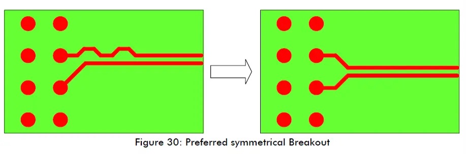
Whenever possible, opt for symmetrical routing to avoid compensating for length differences with serpentine traces.

If space allows, consider adding small return loops at the source of short differential traces to compensate for length, rather than using serpentine High-Speed signal PCB routing.