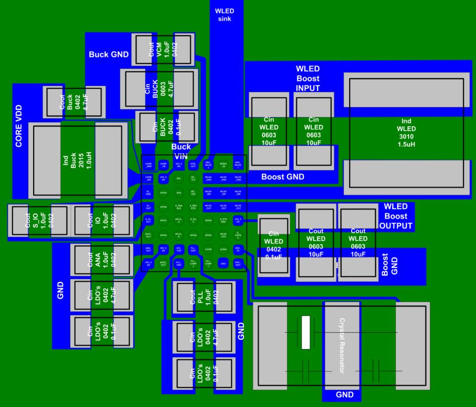
The importance of PCB layout affects the printed circuit board to determine the manufacturing, installation and subsequent maintenance costs of the printed circuit board to a certain extent. In the trend towards higher density electronic designs, the PCB layout and wiring of each electronic product is particularly important. PCB wiring design can often achieve higher layout rates, reduce jumper distribution, electromagnetic interference between connections, and effectively reduce noise generation.
Over the years, PCB seems to be ‘downgraded’ in the field of electronic engineering, becoming an anonymous hero who only works quietly behind the scenes. Managers think that PCB wiring is a trivial manufacturing problem, not a design engineer needs to be concerned about; but as digital circuits become faster and faster, RF circuits are also put into the PCB, the circuit board has become a limiting factor in many designs. While computer-aided design (CAD) tools can help engineers design circuit boards, CAD's automatic wire-wrapping feature often creates more problems...
As with all new technologies, it took a long time for engineers to accept and promote printed circuit boards (PCBs). In the 1960s, the old American electronics company Zeneth was advertising their use of point-to-point wiring. Now, almost all electronics are made from PCBs.
But over the years, PCBs seem to have been ‘downgraded’ in the field of electronic engineering, becoming unsung heroes who work quietly behind the scenes. Managers think that PCB routing is a trivial manufacturing issue, not something that design engineers need to be concerned about;but with digital circuits changing faster and faster, and RF circuits being put into PCBs, the circuit board has become a limiting factor in many designs. While computer-aided design (CAD) tools can help engineers design circuit boards,the auto-wrap feature of CAD often creates more problems.

PCB layout
PCBs are at the centre of design work; new ways of designing and building circuit boards are always being sought. While our colleagues in the industry are still discussing the 68020 chip's instruction buffer architecture, they are already talking about board routing procedures and prototyping that can be done overnight.
In my 40 years of electronic design experience, the circuit board has always been the limiting factor in every design project;’ says Massa. ’You shouldn't just make circuit diagrams to get the job done, you have a higher responsibility to see that those diagrams are translated into a product that can be built and sold.
Modern PCBs are not only time killers, they are critical components with precise design requirements; electronic devices are operating at faster and faster frequencies and signal rise/fall times, so PCBs are becoming more and more important. Take a look at the following short stories that actually happened and you'll get some insight.
Printed Circuit Board Stories about Flying Fighters
The design of the radar jamming device for the F-16 fighter. It is understood that some companies may also experience systemic PCB problems. PCB routing is considered a mechanical engineering task, so our electrical engineers throw the schematics to other departments to do the PCB routing.
The printed circuit board I got had a very high-speed emission coupled logic (ECL) oscillator, but the 8-layer circuit board prototype wouldn't work; since there was plenty of room in the circuit board layers, I wondered how they designed it. Smashed. It turns out that in order to simplify the design under the various components of the aluminium heat sink, the mechanical engineers laid out the components according to the shape; the ECL chip is in the top left corner of the board, the resistor in the middle, the crystal on the right, and the bottom corner is exactly 8 inches away from the ECL chip.
From then on, we will make sure that when the mechanical engineer lays out the components on the printed circuit board, there is an electrical engineer next to him who will review the entire layout before it is ready to be manufactured.