Why PCB connected to the board?
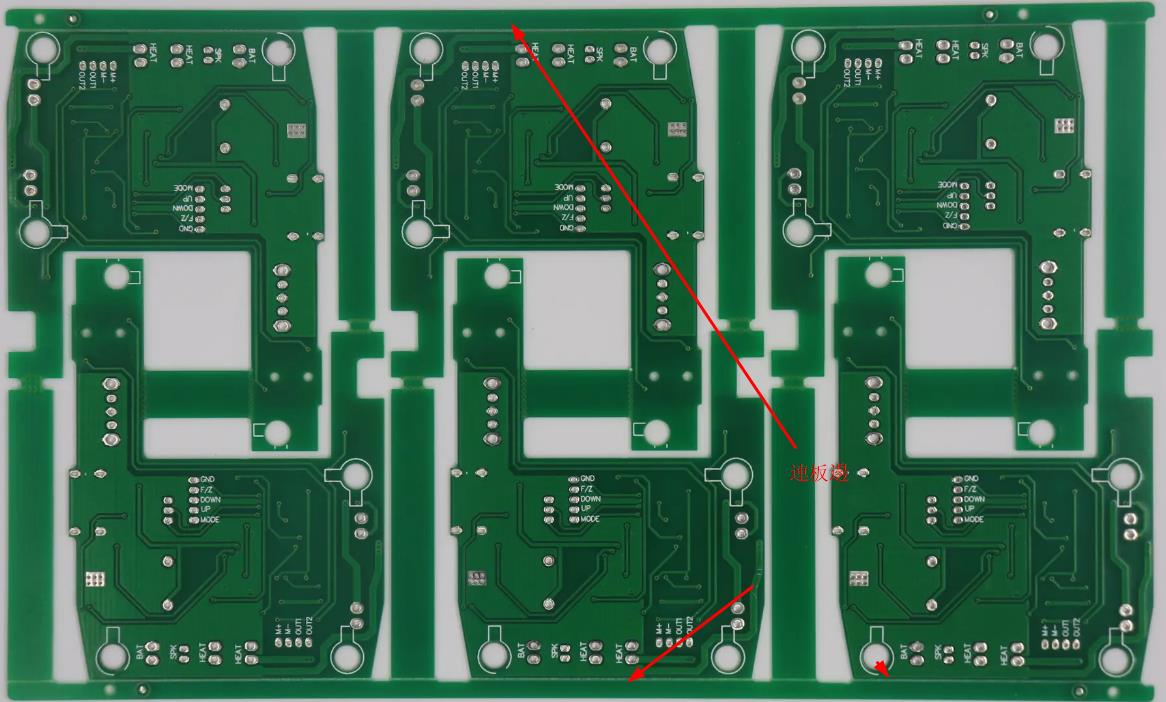
After the completion of PCB design and manufacturing need to be on the SMT assembly line to paste the components, each SMT processing factory will be based on the processing requirements of the assembly line, the provisions of the most appropriate size of the PCB regulations, such as the size is too small or too large, the assembly line to fix the PCB on the assembly line can not be fixed. So the question is, if our PCB size itself is smaller than the size of the factory to give the provisions of what to do? That is, we need to connect the PCB board, the PCB into a whole piece. The board assembly can significantly improve the efficiency of both high-speed punching machine and wave soldering.
Explanation of the term PCB connected to the board
Before we explain how to do it, let's explain a few key terms first.
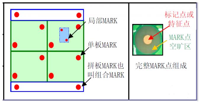
Mark point: as shown in the picture below

Mark Points for PCBs
Mark points are used to help the optical positioning of the punch machine has at least two asymmetric datum points on the diagonal of the PCB board of the punch device, the whole PCB optical positioning datum point is generally in the whole PCB diagonal corresponding position.The datum point for optical positioning of the whole PCB is generally at the corresponding position of the diagonal of the sub-piece PCB.For QFP (Square Flat Packaging) with lead spacing ≤0.5mm and BGA (Ball Grid Array Packaging) with ball spacing ≤0.8mm, in order to improve the accuracy of punching, it is required to set the reference points at the two diagonal corners of the IC.
Requirements for datum point
1.The preferred shape of the datum is a solid circle.
2.The dimension of the datum is 1.0 + 0.05mm in diameter.
3.The datum is placed in the effective PCB range, the centre is more than 6mm from the board edge.
4.In order to ensure that the printing and typing of the identification of the effect, the reference mark near the edge of the 2mm range should not be any other silkscreen logo.Solder pads, V-grooves, stamp holes, PCB boards.Stamp holes, PCB board notches and alignments.
5.Benchmark pads.Soldermask setting is correct.
Considering the contrast between the data colour and the environment, leave a non-resist area 1 mm larger than the optical positioning datum, and do not allow any characters, and do not require the design of metal protection ring outside the non-resist area.
The PCB board edge (process edge) is to assist the production insert to go to the board.Soldering over the wave crest on the two sides or four sides of the PCB board new parts, mainly to assist the production, does not belong to a part of the PCB board, the production is completed to be removed.

Board Edge
V-groove
V-groove is suitable for PCBs with straight line separation edges, such as rectangular PCBs. after opening the V-groove, the remaining thickness X should be (1/4~1/3) of the board thickness L, but the minimum thickness X should be ≥0.4mm.The upper limit can be taken for the boards with heavier load bearing, and the lower limit can be taken for the boards with lighter load bearing. The misalignment S of the V-groove upper and lower cuts should be less than 0.1mm. Due to the limitation of the minimum effective thickness, it is not suitable to use V-groove with board piping for boards whose thickness is less than 1.2mm. If it is necessary to process V-grooves, the V-groove processing requirements must be stated on the processing sheet.
PCB Stamp Hole
PCB stamp hole setting requirements: When the stamp hole is connected with the process side and no guide wire is threaded in the middle, the setting requirements are as shown in Fig. 2.5-a; When the stamp hole is connected with the process side and guide wire is threaded in the middle, the setting requirements are as shown in Fig. 2.5-b, which requires that the guide wire on both sides of the hole is not routed in the same layer, and the width of the wire is 0.3mm; When the two connecting boards are connected, such as when the V-groove is not used, the setting requirements are as shown in Fig. 2.5-c; The above three kinds of connecting pipelines are as follows The distance between two neighbouring connecting keys is required to be between 6 mm and 40 mm.

PCB Stamp Hole
PCB Description
Dimension
a. In order to facilitate processing, the corners of the single board or process edges should be R-type chamfering, the general diameter of the rounded corners is Φ 5, small boards can be adjusted appropriately.
b. When the size of the single board less than 100mm × 70mm PCB should be connected to the board (see Figure 3.1).
PCB size requirements
Length L:100mm ~ 400mm Width W:70mm ~ 400mm
Irregular PCB
PCBs with irregular shapes and not connected to the board should be processed with art edges. If there are holes larger than 5mm × 5mm on the PCB, the holes should be made up first in the design to avoid diffuse tin and board deformation caused by soldering, and the made-up part and the original PCB part should be connected by a few points on one side, and then be removed after wave soldering.
When the connection between the craft edge and PCB is a V-groove, the distance between the outer edge of the device and the V-groove should be ≥2mm; when the connection between the craft edge and PCB is a stamp hole, the devices and wires are not allowed to be placed within 2mm around the stamp hole.
The direction of PCB connection should be designed parallel to the direction of the transmission edge, except when the dimensions cannot satisfy the above requirements for the layout dimensions. Generally, the number of ‘V-CUT’ or stamp hole lines should be ≤3 (except for long and thin single boards).
When connecting PCBs with shaped boards, attention should be paid to the connection between PCB boards and boards, so that each step of the separation of the connection is on the same line.