In PCB design, "how to calculate resistance in layout design" is a crucial aspect that is directly related to the performance and reliability of the circuit. In order to accurately calculate the resistance in layout design, you need to take into account a number of key factors, including copper resistivity, line width, line length, copper thickness, and the actual current through the size.
Why we need to calculate resistance in layout design?
1. ensure current carrying capacity
Every alignment has a certain resistance. If the resistance of an alignment is too high, it can lead to localized heating and even burning of the line when passing current. Calculating resistance can help design a reasonable line width and copper thickness to ensure that the alignment can safely carry the expected current.
2. control Temperature Rise to Avoid Overheating
The higher the resistance, the more heat (P = I²R) is generated as current passes through. Excessive temperature rise can affect the performance of the PCB material, reducing its lifetime and even leading to electrical failure. By calculating resistance, designers can control heat generation at the source.
3. ensure Circuit Signal Integrity
Especially in high-speed circuits, the resistance of the alignment can affect the signal quality, leading to signal attenuation, timing distortion and other problems. Reasonable control of the alignment resistance helps to maintain signal integrity.
4. preventing Voltage Drop
If the resistance in layout design is too high, it may cause a voltage drop across the terminals in high-current applications, affecting circuit function. Therefore, calculating the resistance in advance can prevent potential problems.
5. meet design specifications and safety standards
Many industry standards (e.g., IPC-2221) have specific requirements for alignment width, current density, and temperature rise. By calculating the resistance, you can verify that the design meets the specification and avoid rework or failure at a later stage.

how to calculate resistance in layout design
How to calculate resistance in layout design?
1. determine the basic parameters
First of all, the resistivity (ρ) of copper needs to be specified, which usually takes a value between 1.65×10-⁸ Ω•m and 2×10-⁸ Ω•m.
Next, determine the line width and length. Line width is usually measured in mils (mils), 1 mil = 0.0254 mm. Copper thickness is usually expressed in ounces (oz), and a common 1 oz copper thickness is about 35 μm (microns).
2. calculate the cross-sectional area
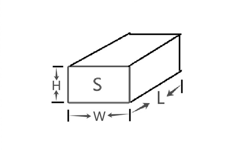
Cross-sectional area (S) = line width (W) × copper thickness (H).
In the calculation, pay attention to the unity of the unit, usually the line width and copper thickness is converted to meters (m).
3. how to calculate resistance in layout design
resistance (R) = ρ × L / S, where L is the wire length, S is the cross-sectional area.
Again, the wire length L needs to be converted to meters (m), and the final resistance unit is ohms (Ω).

calculation of resistance
4. consider the effect of temperature on resistance
Temperature changes affect the resistivity of copper. As the temperature rises, the thermal vibration of positive ions within the metal increases, and the hindrance to free electrons increases, resulting in a rise in resistance.
Typically, the resistivity of copper increases by about 0.004% (40 ppm/°C) for every 1°C increase. In practical applications, especially in high current or high temperature environments, this change must be fully considered.
5. focus on current density
Current density (J) = Current (I) / Cross-sectional area (A).
In high current applications, high current density may lead to local overheating. Therefore, the current density needs to be reasonably controlled in the design stage to ensure the thermal stability and reliability of the line.
6. optimization in practical applications
In the actual design, it may be necessary to adjust the alignment width or copper thickness according to the current size, temperature rise requirements and other factors. Online calculation tools or professional software can be used to optimize the parameters more accurately.
7. follow the design specifications
In the calculation of resistance and layout design, should follow the relevant PCB design specifications, such as line width standards, current carrying capacity requirements, etc., in order to ensure the safety and stability of the final circuit.
8. testing and verification
After the completion of the design, the electrical performance of the alignment should be verified through actual testing to ensure that the resistance meets the expected requirements to further improve product reliability.
Through the above steps, you can systematically calculate and optimize the resistance in layout design to provide reliable protection for circuit design.