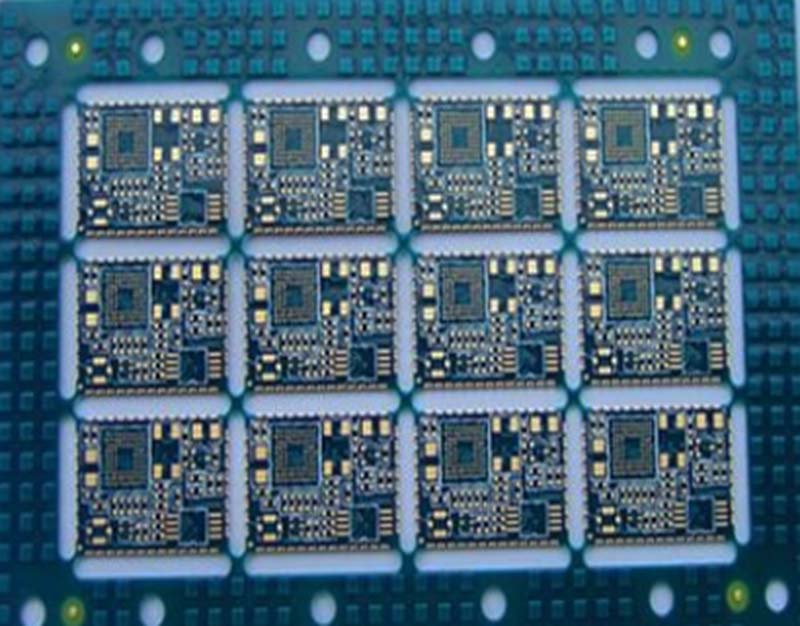
IC board, also known as package substrate, is the connection and transmission of the bare chip (DIE) and the printed circuit board (PCB) between the signal medium, can be regarded as a high-end PCB products.
IC board's main responsibility is to protect the circuit, stable line and dissipate the excess heat, which is the core component of the packaging process, the proportion of the cost of the low-end package is 40-50%, and in the high-end package is It is the core component of the packaging process, accounting for 40-50% of the cost in low-end packaging and 70-80% in high-end packaging. In the field of advanced packaging, IC carrier board has replaced the traditional leadframe.
Compared with PCB, IC board has higher requirements in technology, the technology of IC board originates from HDI (High Density Interconnect) technology, from ordinary PCB to HDI, then to SLP (class carrier board), and finally to the IC board, its processing accuracy is gradually improved. Unlike the reduction method used for traditional PCBs, IC boards are mainly manufactured using processes such as SAP (Semi-Additive Process) and MSAP (Modified Semi-Additive Process), which require different equipment and higher processing costs, as well as more precise parameters such as line width/space, board thickness, aperture, etc., and higher requirements for heat resistance.
①Brightening agent (also known as accelerator), whose function is to reduce the polarisation effect, accelerate the deposition of copper and refine the grain;
② Wetting agent (also called retardant) can enhance cathodic polarisation, reduce surface tension and assist the brightening agent to play a role;
③ levelling agent can inhibit the deposition of copper in the high current density region.
Micro-blind pore bottom and pore deposition rate differences, the root cause of the additives in different locations in the pore adsorption distribution is not uniform. The distribution formation process is as follows:
① The levelling agent is most likely to be adsorbed in the region with the most negative potential at the pore opening because of its positive charge. Because of its relatively slow diffusion rate, the concentration of levelling agent gradually decreases at the bottom of the pore.
② The accelerator tends to be enriched in the low current density region, and its diffusion rate is faster, resulting in a gradual increase in the concentration of accelerator at the bottom of the pore.
③ In the region where the hole potential is most negative and the convection is most intense, the levelling agent will gradually replace the inhibitor, thus strengthening the inhibition of the hole.
The process of electroplating hole filling can be divided into the following three stages:
① Additive adsorption equilibrium stage. In this stage, the concentration of brightener at the bottom of the hole gradually accumulates, and the adsorption of levelling agent at the hole mouth also gradually increases, forming the difference between the concentration of additives inside and outside the hole, and maintaining a dynamic equilibrium state.
② Hole filling burst stage. This stage of the hole deposition rate is rapidly accelerated, while the hole deposition rate is relatively slow, showing a ‘bottom-up’ (bottom-up) filling trend.
③ Post-filling pore modification stage. In this stage, the Dimple is further reduced and the hole pattern is modified in detail.

Substrate structure: Multi-layer stacking design, consisting of alternating layers of conductive and non-conductive materials of different thicknesses; penetration holes, i.e. holes used to realise signal interconnections between different layers. The structure specifically includes:
Via Hole (same as ‘drill hole’) for electrical connection between layers;
Via Land, the open area surrounding the Via Hole;
Hole Wall, which forms the inner wall of the Via Hole;
Hole Cap, the structure used to close the top of the via;
Plugging Ink, the material used to fill the inside of the via.
In addition, there are Surface Treatment (Surface Treatment) processes, including:
Electro-gold plating (EG), where a layer of gold is plated on the surface;
Ni thickness, which specifies the thickness of the nickel layer;
Au thickness, which specifies the thickness of the Au layer.
Key challenges in substrate processing:
Layer structure capability, i.e., the ability to fabricate the laminated structure of the substrate;
Pattern alignment capability (Trace/Pattern capability), which refers to the production accuracy of the line pattern on the substrate;
Fingerpitch capability (Fingerpitch capability), that is, the spacing between the gold finger control capability;
Soldermask alignment capability (CF/SM registration capability), which involves the alignment accuracy of the soldermask layer and the line layer;
Drill capability, which refers to the accuracy and efficiency of drilling holes in the substrate;
Surface treatment (Surface treatment), involving the substrate surface plating or treatment process;
Dimension tolerance control capability (Dimension tolerance capability), that is, the substrate processing process of dimensional tolerance control capability.
As a core component of high-end packaging, the processing technology and process requirements of IC board are extremely high. From additive adsorption to substrate structure design, every step is critical. In the face of processing challenges, manufacturers need to continuously upgrade their technologies to meet market demands. In the future, IC board technology will continue to develop and help the electronics industry progress.