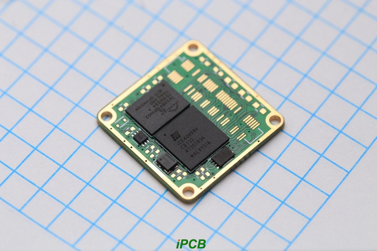
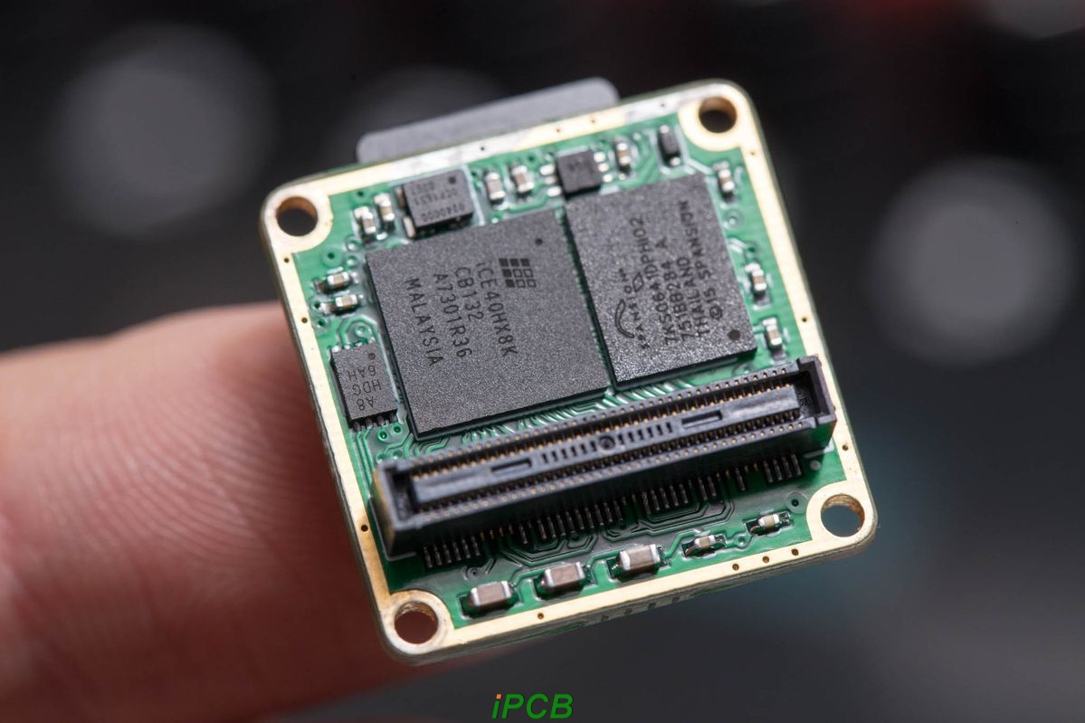
As technology becomes smaller and faster, the components inside our devices also need to keep pace. This is the origin of IC substrates (PCBs). IC substrates (packaging substrates) possess a series of excellent characteristics such as high density, high precision, high performance, miniaturization, and thinness, making them an indispensable key component in modern electronic products. They help connect microchips to the main circuit board while saving space and improving performance. At the same time, IC substrates also have high temperature and high frequency resistance, enabling them to support the high-speed computing and data processing needs of future electronic devices. IC substrates (PCBs) connect chips to the motherboard of compact, high-speed devices. It should be noted that IC substrates and PCBs are not the same concept.

In the 1970s, the demand for electronic devices began to show a trend towards miniaturization, low cost, and high performance, driving the application of organic packaging materials. At this stage, ceramic and metal substrates, while possessing good thermal conductivity and mechanical strength, had high processing costs and were heavy, hindering miniaturization and mass production. Organic materials (such as epoxy resin) offered advantages such as light weight, ease of processing, and low cost, becoming an ideal alternative. Organic IC substrates were initially developed from printed circuit board (PCB) technology, borrowing commonly used organic materials in PCBs, such as FR-4 and polyimide (PI).
Comparing IC substrate PCBs to traditional PCBs, the differences go beyond just size. We break it down into four key aspects: density, size, performance, and reliability.
Smaller and More Compact
IC substrate PCBs are designed for small devices. They can integrate more connections, microvias, and thinner layers in a smaller space. This makes them ideal for smartphones, wearable devices, and micro-sensors. Traditional PCBs are bulkier and not space-saving.
Faster and Better Performance
These boards are designed for high-speed signals. With better impedance control, they maintain stable and fast signals—ideal for 5G and artificial intelligence. Traditional PCBs cannot handle both speed and precision simultaneously.
More Efficient Heat Management
IC substrate PCBs are better at dissipating heat from the chip. They use special materials and have ventilation holes that keep the device cool even under high loads. Traditional PCBs typically require additional components for heat dissipation.
More Reliable, Handling Tough Work: Because they are made with high-end materials and carefully tested, IC substrate PCBs have a longer lifespan and perform better in harsh conditions—such as automotive, aircraft, or medical devices. Ordinary PCBs are robust, but cannot meet the same high demands.

Types of IC Substrate PCBs: Not all IC substrate PCBs are the same. They vary in form, depending on the packaging method, the materials used, and the way the chip is bonded. Let's take a closer look.
Semiconductor Packaging:
BGA (Ball Grid Array): This type handles a large number of pins. It also performs well in thermal control and electrical performance. It is typically used in situations requiring both compact size and robust connections.
CSP (Chip-Scale Package): CSPs are very small—almost the same size as the chip itself. They are ideal for mobile devices, memory chips, and other applications where space saving is critical.
Flip Chip (FC): In this device, the chip is flipped over and directly attached to the substrate. This helps reduce signal interference, supports faster speeds, and improves heat dissipation.
MCM (Multi-Chip Module): MCMs integrate multiple chips into a single package. They save space and reduce weight, but may not offer optimal thermal or signal performance compared to other types.
By Material Type:
Rigid: Made from materials such as epoxy, BT resin, or ABF, rigid substrates are most commonly used. They offer a good balance of stability and performance.
Flexible: Flexible substrates use PI or PE resin, allowing the board to be bent or folded. These are ideal for wearable devices, foldable phones, or space-constrained applications.
Ceramic: Made from materials such as alumina (Al₂O₃) or aluminum nitride (AlN), ceramic substrates offer excellent thermal control and high reliability, especially in harsh environments.
By Bonding Technology:
Wire Bonding: A traditional method that uses fine wires to attach the chip to the substrate. This method is simple, cost-effective, and suitable for many applications.
TAB (Automated Tape Bonding): Uses flexible tape to bond the wafer. This method is faster and more accurate, especially suitable for automated production.
Flip Chip Bonding: Uses bumps or solder balls to connect the wafer face-down. This method supports high-density interconnects and is ideal for performance-critical designs.
The core of the IC substrate fabrication process includes several key steps, each crucial to ensure the high quality and reliability of the final product.
Vacuum Lamination: First, the add-on adhesive film is vacuum-laminated to the core board. This step requires specific temperature and pressure conditions to ensure a tight bond. A hot press is typically used to fully fuse the add-on adhesive film to the core board under precisely controlled conditions, forming a stable base structure. Good lamination quality is crucial for the success of subsequent processes.
Laser Drilling: Next, micro-holes are formed using laser drilling technology. This process utilizes a high-energy laser beam to precisely drill holes, achieving micron-level apertures without damaging the material. The key lies in the precise control of the laser's focus and movement speed, ensuring accurate hole diameter and position, and smooth hole walls, laying a solid foundation for subsequent chemical processing.
Removal of Adhesive Residue: After drilling, adhesive residue is removed to clean the hole walls. This step typically uses chemical solvents or ultrasonic cleaning to ensure no residue remains inside the hole. Residue not only affects conductivity but can also lead to circuit defects, making thorough cleaning crucial.
Seed Layer Formation: Next, a conductive seed layer is formed using chemical copper plating or sputtering techniques. This process requires strict monitoring of the chemical concentration, temperature, and reaction time to achieve a uniform plating thickness. The quality of the seed layer directly affects the subsequent electroplating effect and is fundamental to ensuring good conductivity.
Electroplation Thickening: Then, an electroplating process thickens the circuitry and fills the micropores formed by laser drilling. During electroplating, current density and time must be controlled to ensure the uniformity and thickness of the plating layer. This step is critical, ensuring the integrity of the conductive path while providing sufficient mechanical strength.
Dry Film Removal: Next, the dry film is removed, clearing away excess material. This step is typically performed using chemical solvents to remove the protective film covering the circuit, exposing the electroplated conductive lines and ensuring the clarity and accuracy of the circuitry.
Flash Etching: Finally, excess seed layers are removed through flash etching. Flash etching is a selective removal technique that uses appropriate chemicals to remove only the seed layers not covered by electroplating. This step ensures the purity of the circuit while improving the electrical performance of the product.
Throughout the process, the key challenge lies in precisely controlling the chemicals and process parameters at each step to ensure the formation of high-precision conductive interconnects, especially during seed layer formation and microvia filling.
The process must be highly precise to ensure electrical performance and structural integrity. Due to these characteristics, this packaging substrate technology has wide applications in advanced packaging, particularly for high-density packaging needs such as high-performance computing, 5G communications, and artificial intelligence devices, driving electronic products towards higher performance and smaller size.
Fabricating IC substrate PCBs is more difficult than manufacturing ordinary PCBs. These boards are very thin and require a high level of accuracy.
IC substrate PCBs play a crucial role in today's advanced electronic products. They enable the manufacture of smaller, faster, and more powerful devices. With their robust performance, reliability, and thermal control, they are a wise choice for many high-tech applications. If you are looking for a partner to handle IC substrate PCBs, iPCB is here to assist you. We specialize in high-precision IC substrate PCB manufacturing and are ready to support your next project with high-quality, fast, and professional service.