PCB impedance matching is commonly encountered in the design of multi-layer PCBs, where various high-frequency signals such as RF and antenna are used for impedance control to ensure the stability of the PCB and the pass rate of various indicator tests.
impedance matching
To distinguish the resistance of direct current (DC), the resistance encountered by alternating current is called impedance (Z0), which includes resistance (R), inductance (XC), and capacitance (XL).
PCB characteristic impedance is also known as "characteristic impedance". It refers to the resistance of high-frequency signals or electromagnetic waves in the transmission signal line (i.e. PCB copper wire we manufacture) relative to a certain reference layer (i.e. shielding layer, projection layer or reference layer) at a certain frequency, which is called the characteristic impedance during propagation. It is actually the sum of vectors such as resistance, inductance, capacitance, etc.
Various signals are transmitted in the conductors of PCBs, and in order to improve their transmission rate, it is necessary to increase their frequency. If the circuit itself is affected by factors such as etching, layer thickness, and wire width, it will cause changes in impedance values, leading to signal distortion. Therefore, the impedance value of a conductor on a high-speed PCB should be controlled within a certain range, which is called impedance matching.

impedance matching
The significance of controlling PCB characteristic impedance
PCB not only plays a role in current conduction in electronic products but also in signal transmission.
The high-frequency and high-speed PCB of electronic products requires that the circuit performance provided by the PCB must ensure that the signal does not reflect during transmission, and that the signal is intact and not distorted.
PCB characteristic impedance is the core of solving signal integrity problems
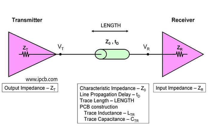
When operating electronic devices (such as computers, communication switches, etc.), the signal emitted by the driver must reach the receiver through the PCB signal line. To ensure signal integrity, the characteristic impedance (Z0) of the PCB signal line must match the electronic impedance of the head and tail components.
When the rise time of the transmission line exceeds 1/3, the signal will reflect, so the PCB characteristic impedance must be considered.
Factors affecting the characteristic impedance
The dielectric constant of a PCB is inversely proportional to its characteristic impedance (ER)
The dielectric thickness between the PCB circuit layer and the ground plane (or outer layer) is directly proportional to the characteristic impedance value (H)
PCB impedance line bottom width (W1 below). The width of the line surface (upper W2) is inversely proportional to the characteristic impedance
PCB copper thickness is inversely proportional to PCB characteristic impedance (T)
The distance between adjacent PCB lines is directly proportional to the characteristic impedance value (differential impedance) (s)
The thickness of the solder mask layer on the PCB substrate is inversely proportional to the impedance value (c)
Process factors affecting PCB impedance matching
Due to etching, the impedance of the PCB cannot be controlled when the thickness of copper exceeds 2oz.
There is no copper wire layer blank in the design, and solidification sheets need to be filled during production. When calculating impedance, it is not possible to directly replace the dielectric thickness provided by the sheet supplier, but rather to subtract the thickness of the blank area filled with the curing sheet. This is one of the main reasons why our calculated impedance is inconsistent with the manufacturer's results.
So how do we control PCB impedance matching in our design?
1. Record the impedance lines previously made using empirical values, such as the line width and board thickness of the PCB, and apply them directly to the next use.
2. Firstly, according to the conventional design, highlight the circuit that requires impedance in the PCB, and then take a screenshot to provide to the PCB factory. If the PCB factory wants to control it, they will modify the data according to the PCB impedance we need, such as adjusting the PCB line width and line spacing to achieve the required impedance.
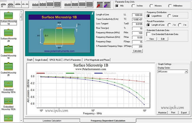
3. At the beginning of the design, based on the lamination parameters of the PCB and the relevant data provided by the PCB manufacturer (PCB board, dielectric constant, green oil, PP thickness, etc.), we used Si9000 software to calculate impedance and then used the calculated parameters to track the impedance line, ultimately obtaining PCB data. At the same time, the PCB factory needs to control the impedance of the PCB. The advantage of doing this is that PCB factories generally do not manipulate our data, which is also a small adjustment.

PCB impedance calculation
PCB impedance calculation
The calculation of impedance matching is quite cumbersome, but we can summarize some empirical values to help improve computational efficiency. For commonly used FR4 and 50ohm microstrip lines, the line width is generally equal to twice the thickness of the medium. For a 50ohm strip line, the line width is equal to half of the total thickness of the medium between two planes. This can help us quickly lock in the linewidth range. Please note that the calculated line width is less than this value.
In addition to improving computational efficiency, we also need to improve computational accuracy. Do you often encounter situations where your calculated PCB impedance is inconsistent with the PCB factory? Some people may say that this has nothing to do with it. Let the PCB factory make direct adjustments. But will there be a PCB factory that cannot adjust, allowing you to relax PCB impedance control? It is better to do the product well or to have everything under one's control.
When voltage and current propagate in transmission lines, inconsistent characteristic impedances can cause so-called signal reflection phenomena. In the field of signal integrity, issues such as reflection, crosstalk, and power plane cutting can all be classified as impedance discontinuity problems, so the importance of matching is demonstrated here.
We summarize the impedance knowledge of PCBs as follows:
1. The function of impedance is to ensure the integrity of signal transmission, ensuring that the signal can be fully transmitted from point A to point B without deformation or distortion.
2. Impedance matching is mainly required for high-speed signals.
3. The impedance matching values of different signals are different, and the PCB design engineer shall confirm them by the requirements of the scheme.
4. The impedance matching value is influenced by many factors of PCB.
5. Impedance matching value is calculated comprehensively through professional impedance matching calculation software, taking into account factors such as impedance type, line width, line spacing, board, stack, board thickness, and medium.
6. PCB manufacturers use equipment such as impedance testers to test whether the final impedance value matches the calculated theoretical impedance value.
We provide free impedance calculation and impedance stacking suggestions. If you need impedance-related inquiries, please feel free to contact us.