In modern high-speed and high-frequency electronic systems, PCB traces can no longer be treated as simple electrical connections. As signal edge rates increase and operating frequencies rise, PCB interconnects behave as transmission lines. Under these conditions, impedance control becomes a fundamental requirement to ensure signal integrity, electrical performance, and system reliability.
Impedance-related issues such as reflections, ringing, overshoot, eye diagram closure, and electromagnetic interference (EMI) are commonly observed when impedance is not properly controlled. These problems are especially critical in applications such as communication equipment, data centers, automotive electronics, industrial control, and aerospace systems.
1. Why Impedance Control Is Required
Impedance control is required whenever the signal rise time is comparable to, or shorter than, the propagation delay of the PCB trace. In such cases, impedance mismatches along the signal path cause partial signal reflections, which distort the waveform and degrade timing margins.
Typical consequences of poor impedance control include:
Signal reflection and ringingIncreased jitter and timing uncertainty
Crosstalk between adjacent traces
EMI and compliance failuresReduced system reliability
For high-speed digital interfaces and RF signals, impedance control is not optional—it is a basic design and manufacturing requirement defined by the IC vendor or industry standards.
2. Types of Impedance in PCB Design
PCB impedance control generally involves several different impedance types, depending on the signal structure:
2.1 Single-Ended Impedance
Single-ended impedance refers to the characteristic impedance of an individual trace referenced to a ground or power plane.
Common target values include 50Ω and 60Ω, widely used in RF circuits and high-speed digital signals.
2.2 Differential Impedance
Differential impedance applies to a pair of tightly coupled traces carrying complementary signals.
Common values include:
90Ω (USB)
100Ω (LVDS, Ethernet, PCIe)
110Ω (CAN-FD, some industrial interfaces)
Differential impedance depends not only on trace width, but also on the spacing between the two traces.
2.3 Controlled Impedance vs. Nominal Impedance
Controlled impedance means that the impedance is measured and verified during manufacturing, typically with defined tolerance limits (e.g. ±10%, ±5%).
Nominal impedance, on the other hand, is only calculated during design and not physically tested.
3. What Is an Impedance Coupon
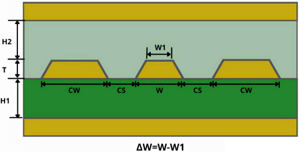
An impedance coupon (also called an impedance test structure) is a dedicated trace pattern placed on the production panel for impedance measurement. It is designed to replicate the actual signal trace geometry as closely as possible, including:
Trace width
Trace spacing (for differential pairs)
Copper thickness
Dielectric structure
Reference plane configuration
Impedance coupons are typically measured using Time Domain Reflectometry (TDR) after PCB fabrication. The measured impedance is then compared with the target value to confirm compliance.
Without impedance coupons, it is not possible to verify real impedance performance in a repeatable and reliable manner.
4. Major Factors Affecting PCB Impedance
The characteristic impedance of a PCB trace is not determined by a single parameter. Instead, it is the result of multiple physical and material factors acting together.
4.1 Trace Width
Trace width has a direct and significant impact on impedance:
Wider traces → lower impedance
Narrower traces → higher impedance
Even small variations in final etched width can lead to noticeable impedance deviation, especially for fine-line designs.
4.2 Dielectric Thickness
Dielectric thickness refers to the distance between the signal trace and its reference plane:
Thicker dielectric → higher impedance
Thinner dielectric → lower impedance
This parameter is strongly influenced by lamination control during PCB fabrication.
4.3 Dielectric Constant (Dk)
The dielectric constant of the laminate material directly affects impedance:
Higher Dk → lower impedance
Lower Dk → higher impedance
It is important to note that Dk is frequency-dependent. The value at 1 GHz may differ significantly from the value at 10 GHz, which must be considered in high-speed and RF designs.
4.4 Copper Thickness
Copper thickness affects impedance by changing the effective trace geometry. Increased copper thickness can lower impedance by increasing the effective conductor size, especially after plating.
4.5 Reference Plane Structure
A continuous and solid reference plane (ground or power) is critical for impedance stability.
Plane splits, voids, or reference changes along the signal path can cause local impedance discontinuities and signal degradation.
4.6 Differential Pair Spacing
This factor applies only to differential signals. The spacing between the two traces directly affects coupling:
Smaller spacing → stronger coupling → lower differential impedance
Larger spacing → weaker coupling → higher differential impedance
Proper balance between trace width and spacing is required to achieve the target differential impedance.
Because all these parameters interact with each other, impedance control must be treated as a system-level design and manufacturing task. Any change to one parameter may require adjustments to others.

5. Impedance Control in Manufacturing
During PCB fabrication, impedance control relies on process stability and engineering compensation, including:
Material selection and consistency
Etching compensation for trace width control
Lamination thickness control
Panel-to-panel process repeatability
Experienced manufacturers use historical process data and impedance modeling to fine-tune production parameters and achieve consistent results.
6. Impedance Measurement and Tolerance
Impedance is typically measured using TDR on impedance coupons. Common tolerance requirements include:
±10% for general high-speed applications
±8% or ±5% for tighter signal integrity requirements
Measured results are documented in impedance test reports and used for quality assurance and customer acceptance.
7. Conclusion
Impedance control is a fundamental requirement for modern PCB design and manufacturing. It is not limited to trace width calculation but involves a comprehensive understanding of materials, stack-up design, fabrication processes, and measurement methods.
By clearly defining impedance requirements, designing appropriate stack-ups, controlling manufacturing variables, and verifying results through impedance testing, reliable signal performance can be achieved in high-speed and high-frequency PCB applications.