What is impedance?In a circuit with resistors, inductors, and capacitors, the resistance to alternating current is called impedance. Impedance is often represented by Z. Impedance is a complex number. The real part is called resistance and the imaginary part is called reactance. The AC current from the capacitor in the circuit to the obstacle is called reactance. The AC current from the inductance in the circuit to the obstacle is called inductance. In the circuit The alternating current caused by the capacitance and inductance of the obstacle is called reactance. The unit of impedance is ohms.
![]()
Impedance calculation formula
We provide free impedance calculations and impedance stacking suggestions.If you need impedance-related consultation, please contact us at sales@ipcb.com
Most electronic engineers have encountered the problem of matching impedance.Generally speaking,the purpose of impedance matching is to ensure that the signal or energy can be effectively transmitted from the signal source to the load.
The most ideal model is of course to hope that the output impedance of the Source end is 50 ohms,the impedance of the transmission line is 50 ohms,the input impedance of the Load end is also 50 ohms, and 50 ohms all the way down, this is the most ideal.
However, the actual situation is: the source impedance will not be 50ohm,and the load end impedance will not be 50ohm.In this case,several impedance circuits are needed.
The matching circuit is composed of inductors and capacitors.At this time,we need to use capacitors and inductors to debug the impedance circuit to achieve optimal RF performance.

Matching impedance
What does impedance mean to PCBs?
As the signal transmission rate of modern electronic circuits increases, the requirements for PCB quality and performance are also getting higher and higher. Only by impedance matching can the circuit performance provided by PCB ensure that the signal remains stable, reflection-free, signal integrity, noise-free, distortion-free, and noise-free during high-speed transmission.Therefore,in the actual production of PCB, strict control of related factors affecting impedance is required.
PCB impedance is widely used in: TV antenna boards, mobile phones, car wireless chargers, computer boards, USB, Ethernet, DDR memory,UnionPay card machines, game console boards, smart home products, communication products, microwave, high frequency, RF board etc.
Without impedance control, considerable signal reflection and signal distortion will occur, leading to PCB design failure. Common signals, such as PCI bus, PCI-E bus, USB, Ethernet, DDR memory, LVDS signals, etc., all have impedance. The impedance ultimately needs to be realized through PCB design, which also places higher requirements on the PCB process. After communication with the PCB manufacturer and the use of EDA software, the impedance of the traces is controlled according to the signal integrity requirements.
Why does PCB need to control impedance?
PCB impedance refers to the resistance and reactance of parameters, and alternating current has a blocking effect. Impedance processing is essential in PCB production.
1. PCB must consider the installation of electronic components. When inserting, issues such as conductivity and signal transmission efficiency must be considered. Therefore, the lower the impedance, the better, and the resistivity should be low.
2. In the process of producing PCB, manufacturing techniques such as copper immersion, electrolytic tin plating (or chemical plating, or thermal spray tin), and connector welding are required, and the materials used in these links must ensure the resistivity of the bottom. In order to ensure the resistance of the circuit board The overall impedance is low and must meet the quality requirements of the product to operate normally.
3. The tin plating process is the most common problem in the entire PCB production and is a key link that affects impedance. The biggest disadvantages of electroless tin plating are that it is easy to discolor (easy to oxidize or discolor), poor welding, which will make it difficult to weld the circuit board, and high impedance, which will lead to poor conductivity or unstable performance of the entire board.
4. The conductors in the PCB will generate various signals. When increasing the transmission rate and frequency, the frequency must be increased. If the lines themselves are different due to factors such as etching, lamination thickness, line width, etc., the resistance will change, causing the signal to change. Distortion leads to a decrease in PCB performance, so the impedance value needs to be controlled within a certain range.

Going through an impedence test
What is an impedance strip?
Impedance Strip = Test Coupon
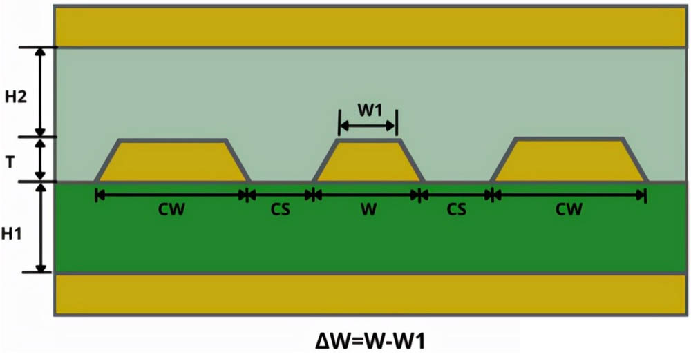
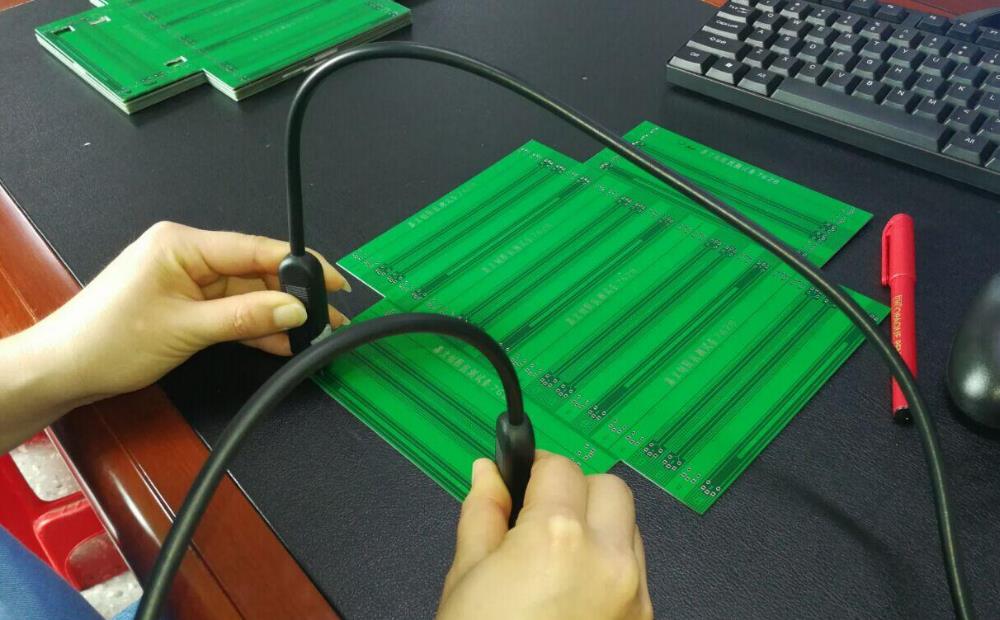
Test Coupon is used to use TDR (Time Domain Reflectometer) to perform impedance testing to see whether the characteristic impedance of the produced PCB meets the design requirements. Generally, the impedance to be controlled is single-ended line and differential pair,so The line width and line spacing of the traces on the test coupon (when there is differential pairing) must be the same as the lines to be controlled. The most important thing is the position of the grounding point during measurement.
In order to reduce the inductance value of the ground lead (ground lead),the grounded place of the TDR probe (probe) is usually very close to the place where the signal is measured (probe tip), so the distance between the point where the signal is measured on the test coupon and the ground point and the pipe must be Comply with the specifications of the probe used.
Impedance types:
1. Characteristic impedance: In electronic information products such as computers and wireless communications, the transmission energy in PCB lines is a square wave signal (called a pulse) composed of voltage and time, and the resistance it encounters is called characteristic impedance.
2. Differential impedance:The driver inputs two identical signal waveforms with opposite polarities, which are transmitted by two differential lines respectively,and the two differential signals are subtracted at the receiving end. Differential impedance is the impedance Zdiff between the two lines.
3. Odd mode impedance:The impedance ZOO of the first line of the two lines to ground is the same.
4. Even mode impedance:The driver inputs two identical signal waveforms of the same polarity, and the impedance when the two lines are connected together is ZCOM.
5. Common mode impedance:The impedance ZOE of one of the two lines to the ground. The impedance values of both lines are the same, usually greater than the odd-mode impedance.
The above is our introduction to what is impedance and impedance types? And why does PCB need impedance matching?The significance of impedance to PCB is explained.