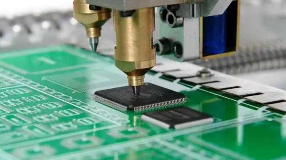
The quality inspection of professional SMT OEM must be very strict, only strict quality inspection can guarantee the quality of SMT OEM products is reliable. After the completion of SMT OEM,quality inspection is a very important part of the processing of poor products can not leave the factory.
Then in the actual production process of processing bad phenomenon of determination is how?Today iPCB share with you some knowledge about the SMT foundry production process.

SMT PCBA
SMT OEM quality terminology
1.Ideal solder joints: good surface wetting, that is, the molten solder on the surface of the metal to be soldered should be spread, and the formation of a complete, uniform, continuous solder cover layer,the contact angle should not be less than 90. The right amount of solder,the amount of solder is sufficient but not too much or too little. Good soldering surface, the surface of the solder joint should be complete, continuous and rounded,but a very bright appearance is not required. Good solder joint position.The position of the component's solder end or pin on the pad is within the specified range.
2.Unwetted:the solder on the solder joint and the metal surface to be soldered to form a contact angle of more than 90 degrees.
3.Open Soldering:Separation of the pad from the PCB surface after soldering.
4.Drawbridge (drawbridging):one end of the component away from the pad facing upwards diagonally or upright,that is, the tombstone (Tomb stone).
5.Bridging:two or more should not be connected to the solder between the solder joints connected,or solder joints of the solder and the neighbouring wires.
6.Void soldering:After soldering,there is sometimes an electrical separation between the solder end and the pad or between the pin and the pad.
7.Pull Tip:The solder in the solder joint has a protruding outward burr,but there is no contact with other conductors or solder joints.
8.Solder ball (solder ball):solder adhesion in the printed board, solder film or conductor on the solder ball, also known as tin beads.
9.Hole: the hole of different diameters at the soldering hole
10.Position offset (skewing):solder joints in the plane of the horizontal,vertical or rotational direction deviation from the predetermined position.
11.Visual inspection method (visual inspection):with the help of lighting 2 to 5 times the magnifying glass,with the naked eye to observe the inspection of the quality of PCBA solder joints.
12.After welding inspection (inspection after aoldering):PCB completed after welding quality inspection.
13. Rework (reworking):To remove the surface assembly components of local defects in the repair process.
14.Patch inspection (placement inspection): surface mount components mounted or after the completion of the leakage of paste,misplaced,paste the wrong,damaged and other cases of quality inspection.
Common NG phenomenon of SMT OEMs
1.Offset Bit:not exceeding 1/4 of the component soldering end (length, width). PCBA processing minimum soldering width (C) shall not exceed the width of the component soldering end (W) or pad width (P) 1/4, calculated according to the lesser of P and W.Maximum offset width (B) shall not exceed the width of the component soldering end (W) or pad width (P) 1/4, calculated according to the lesser of P and W.
2.Less tin: not exceeding 1/4 of the component soldering end (length, width, height).SMT piecework OEM tin height C shall not be less than 1/2 of the component pin height,tin height must be in A and B on the tin height F shall not be less than 1/4 of the height of the component H.
3.Floating height:The height of the soldering surface and PCB pad at the bottom of the component does not exceed 0.5mm.
4.Tin bead: Tin bead diameter is less than 0.1mm.

SMT OEM
Quality control of OEM mounting process
1.SMT components are neatly mounted without offset or skewing.
2.Component model specification is correct, no omission, wrong paste.
3.The components should not be reverse-pasted.
4.Patch devices with polarity requirements must be installed in accordance with the correct polarity label.
Soldering process quality control
1.The surface of the circuit board should be free of solder paste,foreign matter and stains that affect the appearance.
2.The component bonding position should be free of rosin or flux and foreign matter that affects the appearance and soldering.
3.The soldering points under the components should be well formed without abnormal pulling wire or pulling tip.
PCBA board appearance process quality control
1.The bottom of the board,the board surface,copper foil,wiring,through-holes,etc.,should be free of cracks or cuts,no short circuit phenomenon caused by poor cutting.
2.The board should be parallel to the plane,and there should be no bulge or deformation on the board.
3.The board should be free of V/V bias.
4.No blurring, offsetting, reverse printing,offset printing,or ghosting of the silkscreen text of the label information characters.
5.The external surface of the circuit board should be free of expansion and blistering.
6.The aperture size should meet the professional SMT design requirements.
SMT printing process quality control
1.The position of the paste of SMT OEM processing should be centred, without obvious offset,and should not affect the adhesion and soldering.
2.Printing paste is moderate,good adhesion, no less tin, too much paste.
3.The paste point is well formed,there should be no tin, unevenness.
The above is the SMT foundry iPCB to bring you some of the SMT foundry production process of some knowledge, more SMT playing parts foundry technology can be concerned about us.