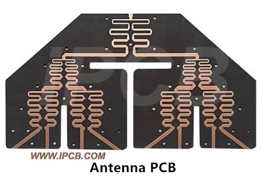
In RF and wireless product design, the dipole antenna is a fundamental and widely used structure due to its simplicity, omnidirectional radiation pattern, and predictable impedance characteristics. Traditionally implemented with wire or rod conductors in free space, the integration of dipole antennas directly onto a printed circuit board (PCB) has become increasingly relevant, especially for compact wireless modules such as IoT devices, BLE, Zigbee, Wi-Fi, and UWB systems.
This article explores the practical aspects of PCB dipole antenna design, the challenges associated with it, and engineering techniques to ensure performance consistency in real-world applications.
1. Why Dipole Antennas on PCBs?
A dipole antenna consists of two symmetrical conductive elements fed at the center. In a typical free-space half-wave dipole, each arm is λ/4 long (where λ is the wavelength at the center frequency), making the total length approximately λ/2.
On a PCB, designers often etch the dipole geometry onto the copper layer, replacing the traditional wire elements. This allows seamless integration of the antenna into the board layout, reducing assembly cost and mechanical complexity.
Key advantages include:
Compact integration in low-profile devices
No need for external antenna components
Cost-efficient mass production
Compatibility with standard PCB fabrication processes
2. Substrate Effects and Effective Wavelength
A critical challenge when designing dipole antennas on PCBs is substrate influence on electromagnetic behavior.
The dielectric constant (εr) of the substrate material affects the effective wavelength (λ_eff), which is shorter than in free space due to wave slowing in the dielectric medium. This leads to:
λ_eff = λ₀ / √ε_eff
Where:
λ₀ = wavelength in free space
ε_eff = effective dielectric constant (typically between 2.2 – 4.5 for FR-4, Rogers, etc.)
As a result, a λ/2 dipole at 2.4 GHz in free space (~62.5 mm total length) may need to be shortened to 40–50 mm when implemented on a standard FR-4 PCB.
3. Impedance Matching and Feed Design
For maximum power transfer and minimal reflection, the antenna impedance must match the RF front-end (typically 50Ω). A dipole antenna in free space ideally exhibits ~73Ω impedance at resonance, but PCB implementation introduces parasitics and detuning effects due to the ground plane and nearby traces.
Common techniques for impedance matching include:
Balun (balanced-unbalanced transformer) circuits
LC matching networks
Microstrip tapers or stubs
Feedline design optimization (coplanar waveguide or microstrip)
Some designers also choose to create a folded dipole structure to raise the impedance to around 300Ω, which can then be transformed to 50Ω using a matching network or integrated balun.
4. Ground Plane and Isolation Considerations
Unlike monopole antennas, which require a ground plane as a mirror image to radiate efficiently, a dipole antenna is a balanced structure and performs best with minimal ground coupling.
However, in PCB design, the presence of a large ground plane can interfere with radiation symmetry, cause impedance mismatch, and distort the far-field pattern.
Best practices include:
Positioning the dipole near the edge of the PCB
Minimizing copper below or near the antenna arms
Using a ground clearance zone around the antenna (e.g., 5–10 mm)
Avoiding signal or power routing under the antenna
In multilayer designs, careful layer stackup planning is critical. Antennas should ideally be on the top layer, away from internal power planes or noisy digital signals.

5. Simulation and Validation
Electromagnetic (EM) simulation tools such as CST Studio, HFSS, or Keysight EMPro are essential for predicting the antenna’s S11 return loss, radiation pattern, gain, and efficiency before committing to hardware.
In particular:
S11 < -10 dB across the desired frequency band is considered a good match.
Radiation efficiency over 30–50% is acceptable for compact devices on lossy substrates like FR-4.
The 3D radiation pattern should meet the application’s coverage needs.
Once fabricated, the antenna should be validated using a VNA (Vector Network Analyzer) and, ideally, in an anechoic chamber to measure actual gain and radiation characteristics.
6. Optimizing Antenna Layout in Compact Enclosures
With increasing demand for miniaturized wireless devices, designers often face severe spatial constraints, especially in wearables, compact IoT modules, and tracking devices. These constraints significantly affect the PCB dipole antenna’s performance.
Key strategies to optimize layout under tight packaging conditions include:
Avoiding high-frequency noise sources: Keep the antenna away from clocks, high-speed interfaces, and power electronics to reduce interference.
Maintaining symmetry: Ensure the two arms of the dipole are as symmetric as possible to preserve balanced radiation patterns.
Utilizing non-electrical areas: Place antenna elements in PCB “dead zones” such as near board edges or between mounting holes.
Considering enclosure effects: Plastic housings or metal shields can detune the antenna; incorporate enclosure models into EM simulations for accurate predictions.
Using flexible PCB extensions: If the main board is too small, the antenna can be designed on a flexible PCB extension folded into available housing spaces.
Vertical stacking: For some designs, stacking antenna elements vertically (along the Z-axis) can improve radiation characteristics and overcome lateral space limitations.
While these constraints cannot be eliminated, careful mechanical and electrical co-design can maximize antenna efficiency and frequency stability within compact products.
Conclusion
PCB dipole antennas offer a practical and compact solution for wireless applications, but their performance hinges on careful attention to material selection, geometry, feed design, and PCB layout constraints. Unlike wire antennas in open space, PCB-based dipoles must contend with lossy substrates, nearby ground planes, and manufacturing tolerances. As such, simulation, prototyping, and testing remain critical to delivering a reliable and efficient antenna system.
Whether you’re designing a simple wireless sensor or a more advanced RF module, mastering dipole integration in PCB layout is a valuable skill that bridges RF theory with practical electronics engineering.