DPC Technology
DPC (Direct Plating Copper) thin film technology is a method of preparing thin films of copper using magnetron sputtering technology.A copper target is placed in a vacuum chamber and a plasma is generated on the surface of the target by magnetron sputtering technology.Ions in the plasma bombard the surface of the target, sputtering it into small particles and depositing them on the substrate to form a thin film of copper.
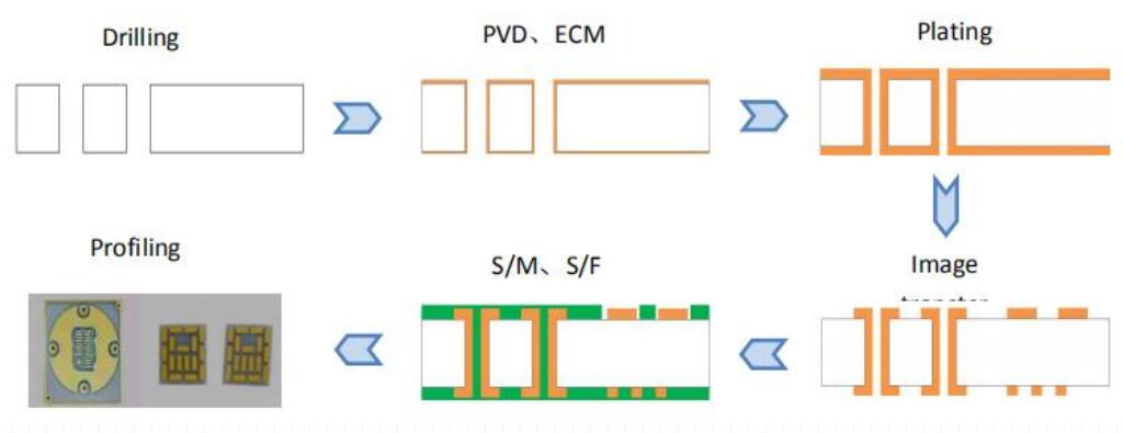
The DPC ceramic circuit board process is based on the thin-film circuit process, where the metallization of the ceramic surface is achieved by magnetron sputtering,and the thickness of the copper layer is achieved by electroplating to a thickness of more than 10 microns.The DPC process pipeline includes vacuum plating, wet plating, exposure developing, etching and other process steps,and the price of ceramic circuit boards for products using DPC technology is relatively high. The DPC process is applicable to most ceramic substrates.
In terms of shape processing, DPC ceramic circuit boards require laser-cutting pipes,which cannot be accurately processed by conventional drilling, milling and punching machines, and therefore, the bonding force and line width are more delicate. Metals have the advantages of good crystallization performance,good flatness,lines are not easy to come off,and the line position is more accurate, line spacing is smaller, and the reliability is stable。
The process of DPC's ceramic circuit boards is as follows:
First use laser to prepare through holes on the ceramic substrate (aperture diameter of 60 μ m ~ 120 μ m,followed by ultrasonic cleaning of the ceramic substrate.Magnetron sputtering technology is used to deposit a metal seed layer (Ti/Cu target) on the surface of the ceramic substrate, followed by photolithography and developing to complete the circuit layer.The metal circuit layer is filled and thickened by electroplating, and the solderability and oxidation resistance of the substrate is improved by surface treatment, and finally the dry film is removed and the seed layer is etched to complete the substrate preparation.
The front end of DPC ceramic substrate preparation adopts transistor microprocessing technology (sputtering coating,photolithography,photolithography, etc.),while the back end adopts printed circuit board (PCB) preparation technology (graphic plating,hole filling,surface grinding,etching,surface treatment), and so on.

DPC Technology
Advantageous features of DPC ceramic substrate
1.Using transistor micromachining technology, the metal lines on the ceramic circuit boards are more delicate (line width/spacing as low as 30 μ m~50 μ m, related to the thickness of the line layer. The DPC ceramic substrate is very suitable for microelectronic devices that require high precision.
2.The use of laser drilling and plating hole filling technology, ceramic substrate vertical interconnection of the upper and lower surfaces, can realize the three-dimensional packaging and integration of electronic devices, reducing the volume of the device.
3.The thickness of the circuit layer is controlled by plating growth (generally 10 μ m ~ 100 μ m.), and the surface roughness of the circuit layer is reduced by grinding to meet the requirements of high temperature and high current device packaging. High current device packaging needs.
4.Low-temperature preparation process (below 300℃). Avoiding the adverse effects of high temperature on the substrate data and metal circuit layer, and at the same time reduce the production cost.
Disadvantages of DPC ceramic substrate
1.The metal circuit layer is prepared by electroplating process, which causes serious environmental pollution.
2.Plating growth rate is low, the thickness of the circuit layer is limited.
3.The bonding strength between metal layer and ceramic is low, the reliability of product application is low.

Ceramic Circuit Board
DBC Technology
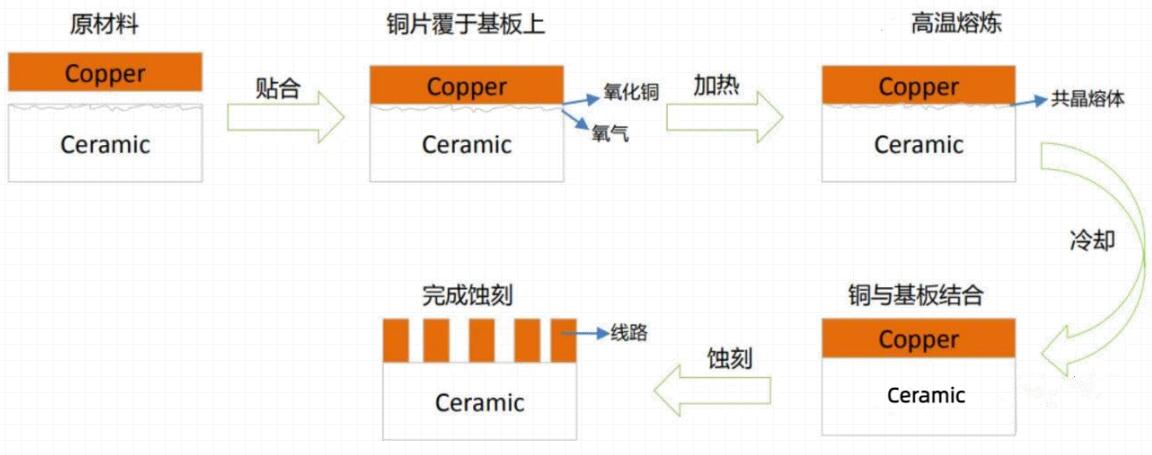
The DBC (Direct Bonding Copper) process is a metallization method that bonds copper foil directly to the surface of an Alumina or Aluminum Nitride ceramic substrate.The basic principle is to introduce oxygen between Cu and ceramics, and then form a Cu/O eutectic liquid phase at 1065-1083°C, which then reacts with the ceramic substrate and Cu foil to form CuAIO2 or Cu(AIO2)2, and bonds the Cu foil to the substrate under the action of the intermediate phase.
DBC ceramic substrate has high graphic precision. Vertical interconnection is possible. Low production cost and other technological advantages, can be widely used in high-power LED lighting. Automobile headlights and other high-power LED field. Semiconductor lasers. Electro-electronic power devices. Microwave. Optical communication, VCSEL, RF devices and other applications, the market space is very large.
Laser is the core component of laser equipment, high power semiconductor laser mainly through the heat sink heat dissipation. Aluminum nitride ceramic heat sink (DBC process) is the mainstream laser heat sink substrate, which can meet the needs of high-power transistor laser wafer bonding in optical communications. High power LED packaging. Semiconductor lasers and fiber optic lasers are widely used in pump source manufacturing. Vehicle-mounted laser radar light source VCSEL to replace the EEL trend, DPC ceramic substrates in high-power VCSEL packaging occupies an important position.

DBC Technologies
AMB Technology
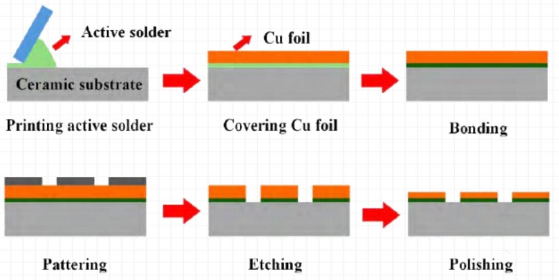
The AMB (Active Metal Brazing) process is a technology that utilizes Ag-based solder containing active elements Ti and Zr to wet and react at the interface between ceramics and metals at a high temperature of about 800°C, thereby realizing heterogeneous bonding between ceramics and metals. Ag-based powders and solder pastes for AMB ceramic substrates are characterized by low oxygen content, high purity and high sphericity.The bonding is realized through the chemical reaction between ceramics and activated metal binder at temperature. Compared with the traditional AI2O3 ceramic substrate,Si3N4 ceramics used in AMB have higher thermal conductivity (>90W/mK25℃) and are closer to the thermal expansion coefficient of silicon (2.6x10 -6/K). The AMB substrate has higher bonding strength and reliability.
AMB ceramic substrate with Ag-based powder and its solder paste products, the product has a low oxygen content, high purity, high sphericity characteristics.
IGBT ceramic liner belongs to the new technology, of which AMB technology ceramic liner is also gradually applied to IGBT modules for new energy vehicles.
IGBT heat dissipation is very important to the performance of the power module, most of the current IGBT module or DBC process. With the working voltage, performance requirements continue to improve, AMB technology ceramic substrate can better solve the above pain points, compared with the DBC, AMB more thermal conductivity, heat resistance, impact resistance, the technology is not only in the automotive field, but also in the aerospace, rail transportation, industrial power grids in the field of extensive application.

AMB Technology
The above introduces the advantages and disadvantages of the three process technologies of ceramic circuit boards,DPC technology,DBC technology and AMB technology, if you need more detailed support, you can contact Audemars Piguet Circuits.