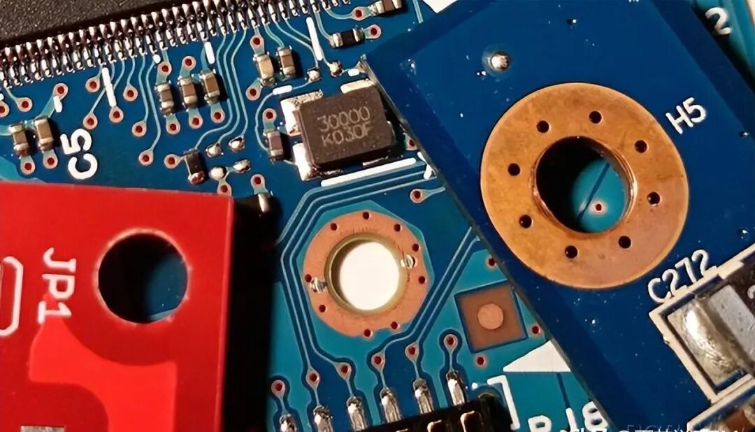
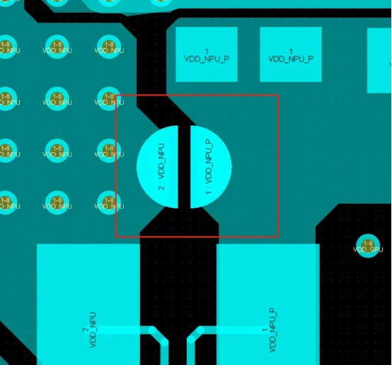
A jumper on a PCB is essentially a metal wire connecting two points on a printed circuit board (PCB). For example, a cable connecting two devices or a network cable connecting switches can be called a jumper. Depending on the product design, the materials and thickness of the jumper vary. Most jumpers are used to transmit voltages at equal potentials, while others are used to provide reference voltage for circuit protection. For applications with precise voltage requirements, even a small voltage drop caused by a metal jumper can significantly affect product performance.
A key performance issue for jumpers is bending performance. Because UTP twisted-pair cables typically have solid cores, they have poor manageability. First, the cables are stiff, making them difficult to bend. Second, solid-core cables exhibit significant return loss when bent, degrading performance. Therefore, solid-core cables generally have specific bend radius requirements. However, flexible, multi-strand cables designed specifically for managing jumpers do not have these issues.
Four major types of jumpers: Which have you used?
1. Copper wire jumpers: Simple and straightforward, but layout interference should be avoided.
2. Resistor jumpers: Stabilize signals, but selecting the right resistance value is crucial.
3. Solder jumpers: Flexible but requires soldering skills.
4. PCB jumpers: Implemented through connection holes, highly flexible.
Three Core Functions of Jumpers
1. Connecting Complex Circuits: Acting like a "circuit matchmaker," solving long-distance component conflicts.
2. Signal Separation: Preventing interference in high-power circuits.
3. Improving Reliability: Reducing failure rates and ensuring a more stable design.
In addition, when PCB design space is limited or routing is already fixed and cannot be modified, adding jumpers to increase current flow is a simple and effective remedy.

Several Common PCB Current Expansion Methods in Hardware Design
Increasing trace width and thickness:
Not only can we increase trace width within a single layer, but when space is limited, we can also widen and thicken the overall trace width by routing traces on different layers. It's important to ensure that more vias are added to enhance heat dissipation, thereby exponentially increasing the current flow.
Exposing copper on the PCB surface (tinning):
Exposing the copper on the trace surface and then tinning it increases the conductor cross-sectional area. This is used in single-sided boards or in situations where the current exceeds the capacity of conventional traces.
Reserving jumpers or copper busbars on the PCB:
Soldering wires or copper strips to the PCB to assist in current carrying. Using copper busbars to carry high current is a common industrial practice, for example in high-power power supplies and server cabinets.

Optimizing stackup design:
Using thicker copper foil (e.g., 2oz instead of 1oz) for power/ground layers improves overall current carrying capacity and is suitable for multi-layer designs. For example, 2oz and 1oz copper foil can handle more current. 2oz copper can also handle higher current. For example, a 100mm wide trace of 2oz copper can handle approximately 10A, while a 1oz copper can handle approximately 5A. This makes 2oz copper ideal for power rails requiring high current. Maintaining the correct trace width is crucial to maximize current capacity and prevent excessive heat buildup.
Using specialized substrates:
such as aluminum-based PCBs, can effectively enhance heat dissipation, thereby increasing the board's overall current capacity.
How to Properly Use Jumper Wires
Although jumpers play a crucial role in PCB design and circuit layout, improper use can also cause numerous problems. Therefore, when using jumpers, please note the following:
1. The length and connection method of jumpers should be as simple and clear as possible; avoid being long or twisted.
2. The position and width of jumpers should be appropriate so as not to interfere with the normal operation of other circuits.
3. The jumper connection should be properly grounded to ensure proper circuit operation.
4. The jumper soldering should be secure and reliable to ensure circuit stability and reliability.
How to Avoid Jumpers on PCBs in Mass Production
1. Optimization During the Design Phase
• Increase the number of PCB layers: If a two-layer board is too tight, switch to a four-layer board and allocate signal/power layers appropriately.
• Perform ERC/DRC checks in advance to confirm electrical connectivity and routing rules.
• Conduct a Design for Manufacturability (DFM) review to discuss production feasibility with the factory in advance.
2. Allow for current margin during layout and routing
• Widen or copper-fill power/ground traces;
• Use multiple parallel traces or copper reinforcement when necessary;
• Avoid using jumpers to increase current after the fact.
3. Synchronize Documents and Projects
• Ensure that the schematic, PCB files, and BOM are completely consistent;
• Maintain clear records of version updates to avoid jumper repairs due to incorrect versions. 4. Rigorous Verification During the Pilot Production Phase
• Perform functional, electrical, and burn-in testing during the pilot production phase;
• If jumpers are necessary, immediately return to the design source and modify the layout before production begins.

Are there any standard guidelines for jumper placement and spacing on PCBs?
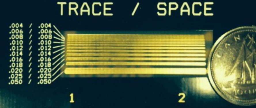
The Institute for Printed Circuits (IPC) provides general guidelines for PCB design and manufacturing, which may indirectly impact jumper-related considerations.
The IPC-2221 series of standards, particularly IPC-2221A, "General Standard for Printed Board Design," provides guidelines for PCB design, including considerations for routing, spacing, and clearance.
IPC-A-600, "Acceptability of Printed Boards," and IPC-A-610, "Acceptability of Electronic Assemblies," provide guidance for inspection and acceptance criteria for PCBs and assembled electronic products. These standards may include criteria for the acceptability of solder jumpers or jumper-related connections.
PCB jumpers are versatile components used in electronic circuits to establish or modify electrical connections on printed circuit boards. Whether it's circuit modification, trace repair, prototype iteration, testing and debugging, design flexibility, or manufacturing efficiency, PCB jumpers offer practical and efficient solutions. By simplifying circuit adjustments and enhancing functionality, jumper on pcb play a vital role in the development, testing, and customization of electronic circuits.