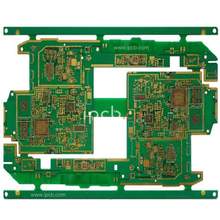
Name:6 layers 1 stage HDI circuit boards
Substrate: FR-4 (ITEQ)
Layer: 6L
Stacking structure: 1+N+1 HDI
Finished board thickness: 1.0m
Copper Plating Thickness: 1oz (35 μ m)
Surface Finish: Chemical Gold
Minimum line width/spacing: 3/3 mil (75 / 75 μ m)
Hole Diameter: Laser Hole = 0.1mm, Mechanical Hole = 0.2mm
Application: Notebook
iPCB's products undergo high-precision automated equipment, product inspection at all levels, and all processes are under strict control. iPCB has been adhering to the ‘relentless pursuit of perfection, wholeheartedly for customer service’ business purposes and ‘professionalism, dedication, honesty, win-win’ business philosophy, continuous self-renewal, improve product quality, improve the company's reputation, and provide customers with a full range of fast, meticulous, rigorous and thoughtful quality service. A full range of fast, detailed, rigorous, thoughtful quality service. We sincerely hope to co-operate with you to establish a long-term mutually beneficial relationship. Welcome to consult and discuss with us to create a win-win situation.

HDI Circuit Boards
Since HDI circuit boards are customised based on customer information, the website is unable to give you an accurate quote.The pictures,processes and prices you see on the website are for reference only.
The actual HDI circuit board price is related to PCB size, process requirements and quantity. Please consult with customer service before placing an order.
Name:6 layers 1 stage HDI circuit boards
Substrate: FR-4 (ITEQ)
Layer: 6L
Stacking structure: 1+N+1 HDI
Finished board thickness: 1.0m
Copper Plating Thickness: 1oz (35 μ m)
Surface Finish: Chemical Gold
Minimum line width/spacing: 3/3 mil (75 / 75 μ m)
Hole Diameter: Laser Hole = 0.1mm, Mechanical Hole = 0.2mm
Application: Notebook
iPCB Circuit provides support for PCB design, PCB technology, and PCBA assembly. You can request technical consultation or quotation for PCB and PCBA here, please contact email: sales@ipcb.com
We will respond very quickly.