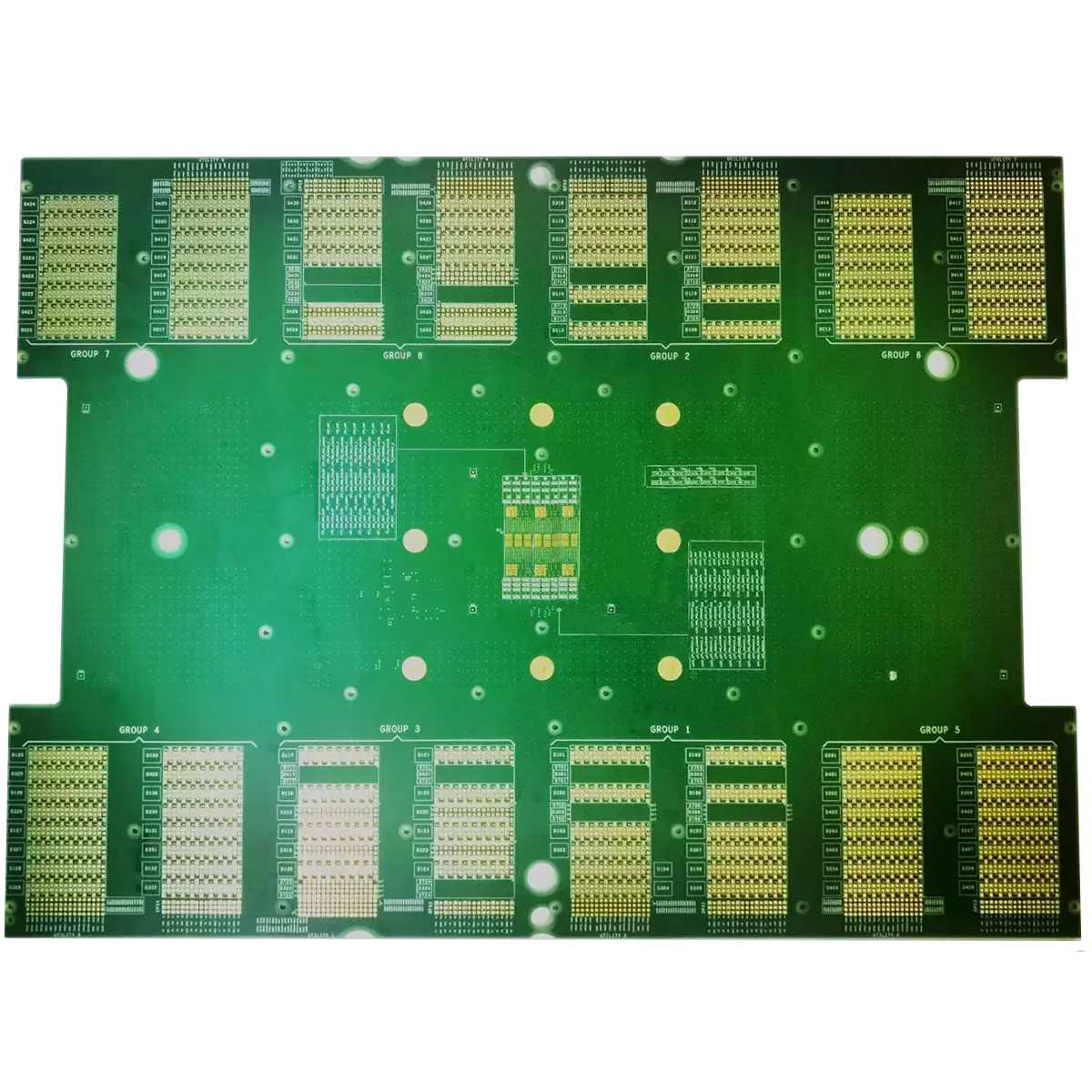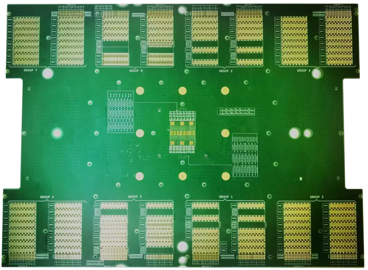
Product name: Load Board
Base plate: TUC/TU872HF
Layer: 56L
Finished size: 20"*22"
Stacking: L1-L56 10mil
L1-L28 12mil
L32-L56 14mil
Surface treatment: Hard gold plating 3-15μ"
Special process: metal edging, fixed depth drilling
Product Application: Wafer Test Board
Load board is a mechanical and circuit interface that connects testing equipment with the device under test. It is mainly used for yield testing after IC packaging in semiconductor manufacturing. Through this stage of testing, defective ICs can be removed, avoiding the scrapping of electronic products due to defective ICs in the future. The test load board is divided into 93K series, T2000 series, TUF series, etc. according to the testing platform.
The semiconductor manufacturing industry includes four major processes: semiconductor design, wafer processing, wafer packaging, and semiconductor testing.
The testing process includes four categories: wafer testing, finished product testing, system level testing, and aging testing. The PCBs involved include Probe card board, Load board, Burn in board (BIB), Interposer board, which are used in conjunction with semiconductor testing equipment. They are customized products that require the production of corresponding PCB according to the chip design for testing purposes.
The demand for semiconductor testing PCB should be released to PCB factory by testing manufacturers, probe card manufacturers, or load board manufacturers. However, due to the complexity of chip design and functionality, as well as the prevalence of fabless mode, there is specialized division of labor in the process of semiconductor chip design and testing. Therefore, the design and procurement of PCBs are not always completed by testing manufacturers, probe card manufacturers, or load board manufacturers. In some cases, semiconductor chip design factories will directly intervene in the entire chip testing process and designate suppliers for the PCBs used for testing. In addition, probe card manufacturers or load board manufacturers may also outsource PCB design services and entrust specialized design companies to complete PCB design and procurement.
Probe card board, load board, and Burn in board belong to multi variety small batch products, while aging board belongs to large batch products. The probe card board, load board, and Burn in board have extremely high requirements for PCB processing technology, and there are few PCB board factories with processing capabilities (the layer design has exceeded 100 layers, the thickness to diameter ratio can reach 40:1 or even higher, BGA can be designed up to 0.3mm, and the appearance requirements are extremely high, resulting in high difficulty and low yield in PCB production.

Load Board
Difference between Load Board and Burn in Board
Load boards are typically used to test the electrical characteristics of semiconductor devices, such as current, voltage, power, etc. It is a bridge connecting the testing equipment and the tested chip, usually including interfaces such as pin sockets, testing points, and power interfaces. The design of the load board must match the pin layout of the tested device to ensure the accuracy and repeatability of the test results.
Burn In Board is used to accelerate the aging process of semiconductor devices and detect their reliability over long-term use. It usually includes a temperature control system for controlling the ambient temperature of the tested device. Burn In Board can also simulate real-world usage conditions, such as high temperature, low temperature, high pressure, and high humidity.
Therefore, the main difference between Load Board and Burn In Board lies in their purposes. Load Board is mainly used to test the electrical characteristics of devices, while Burn In Board is used to test the reliability of devices in long-term use.
Other differences between Load Board and Burn In Board
>Testing time: Load boards are usually used to test newly manufactured devices, and the testing time is relatively short, usually between a few minutes to a few hours. Burn In Board is used for long-term testing, typically requiring several days or even weeks of testing.
>Testing environment: The testing environment of Load Board is relatively simple, mainly the interface between the testing equipment and the tested device, usually without additional control systems. And Burn In Board requires a complete control system, including temperature control, power control, environmental control, etc., to ensure the accuracy and reliability of test results.
>Test accuracy: The Load Board needs to accurately match the pin layout of the tested device to ensure the accuracy of the test results. Burn In Board requires higher testing accuracy to assess the performance and reliability of the device over long-term use.
>Cost: The cost of a Load Board is relatively low, usually requiring only the design of a simple interface to connect the testing equipment and the device being tested. The cost of Burn In Board is relatively high, as it requires more complex control systems and testing equipment, as well as longer testing time.
>Test content: Load Board is mainly used to test the electrical performance of devices, such as current, voltage, power, etc. Burn In Board is mainly used to test the reliability and lifespan of devices, such as aging, stability, and failure rate.
>Testing process: Load Board is usually a one-time test, which can determine whether the electrical performance of the device meets the requirements after one test. Burn In Board requires long-term testing, and the reliability and lifespan of the device can only be determined through analysis of the test results.
>Scope of application: Load Board is suitable for various types of semiconductor devices, including analog devices, digital devices, mixed signal devices, etc. Burn In Board is mainly suitable for high-end and high reliability devices, such as microprocessors, memory, communication chips, etc.
>Management method: Load boards can usually be tested through standard testing procedures and can be easily managed and maintained. And Burn In Board requires more management and maintenance, including regular temperature calibration, power maintenance, environmental control, etc.
>Device type: Load Board is mainly suitable for testing individual devices, such as transistors, diodes, capacitors, etc. Burn In Board is suitable for testing multiple devices, such as memory chips, microprocessors, etc.
>Testing method: Load boards usually use non-destructive testing methods, which means that the testing process will not cause damage to the tested device. Burn In Board, on the other hand, adopts destructive testing methods, which means that the tested device will be damaged to a certain extent during the testing process to simulate the problems that may occur during long-term use of the device.
>Design difficulty: The design of a Load Board is relatively simple, usually only requiring the design of an interface board to connect the testing equipment and the device being tested. The design of Burn In Board is relatively complex and requires consideration of more factors, such as temperature control, power management, testing time, etc.
>Usage scenario: Load Board is suitable for quickly testing newly produced devices to ensure they meet specifications and requirements. Burn In Board is suitable for long-term testing to evaluate the reliability and lifespan of devices and determine their suitability for commercial applications.
>Test data: After load board testing, electrical performance indicators such as current, voltage, power, etc. will be obtained. After Burn In Board testing, reliability and lifespan data will be obtained, such as device aging time, failure rate, MTBF, etc.
>Testing time: The load board testing time is relatively short, usually a few seconds or minutes. And Burn In Board testing takes a longer time, usually several hours or days or even longer.
>Testing environment: Load Board testing requires a relatively stable power supply and testing environment. And Burn In Board testing requires more stringent testing environments, such as constant temperature and humidity chambers, high temperature and high humidity environments, etc.
>Cost: The manufacturing cost of Load Board is relatively low, while the manufacturing cost of Burn In Board is relatively high because it requires more complex design and stricter testing environment.
Load Board and Burn In Board are essential testing tools in the semiconductor industry, with different testing contents, testing processes, applicability, and management methods. Choosing the appropriate testing tools correctly can improve testing efficiency and accuracy, thereby reducing testing costs and improving production efficiency.
Product name: Load Board
Base plate: TUC/TU872HF
Layer: 56L
Finished size: 20"*22"
Stacking: L1-L56 10mil
L1-L28 12mil
L32-L56 14mil
Surface treatment: Hard gold plating 3-15μ"
Special process: metal edging, fixed depth drilling
Product Application: Wafer Test Board
iPCB Circuit provides support for PCB design, PCB technology, and PCBA assembly. You can request technical consultation or quotation for PCB and PCBA here, please contact email: sales@ipcb.com
We will respond very quickly.