LTCC Substrate Circuit Overview
Low temperature co-fired ceramic (LTCC) technology is a multi-layer ceramic manufacturing technology that integrates interconnection, componentless and packaging. With the continuous progress of technology, the appearance of electronic products can now become smaller and thinner, but more powerful. Take the cell phone wireless communications industry, for example, the size of the cell phone shrinks, the early mobile phone function is from the simplest audio broadcast data, has now developed into a handheld network computer. If part of the passive components can be integrated into the substrate, it is not only conducive to the miniaturization of the system, increase the circuit assembly density, but also help to improve the reliability of the system. Current integrated packaging technology mainly includes thin-film technology, silicon semiconductor technology, multi-layer circuit board technology and LTCC technology. LTCC technology is a low-cost packaging solutions, with a short development cycle. Low temperature co-fired ceramic technology can meet the latter's needs of light, thin, short and small. However, low-temperature co-fired ceramic substrates are characterized by high hardness and fragility. Therefore, when the cutting machine cuts hard substrates, the substrate and the cutting blade will generate greater friction between the friction generated by the stress will be transferred to the cutting blade.
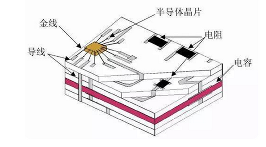
LTCC Substrate Processing Technology
Figure 2 shows the flow chart of LTCC substrate manufacturing process, mainly including mixing, casting, punching, hole filling, screen printing, lamination, isostatic pressure, sintering, etc. The following is a brief introduction to the main processes of each process.
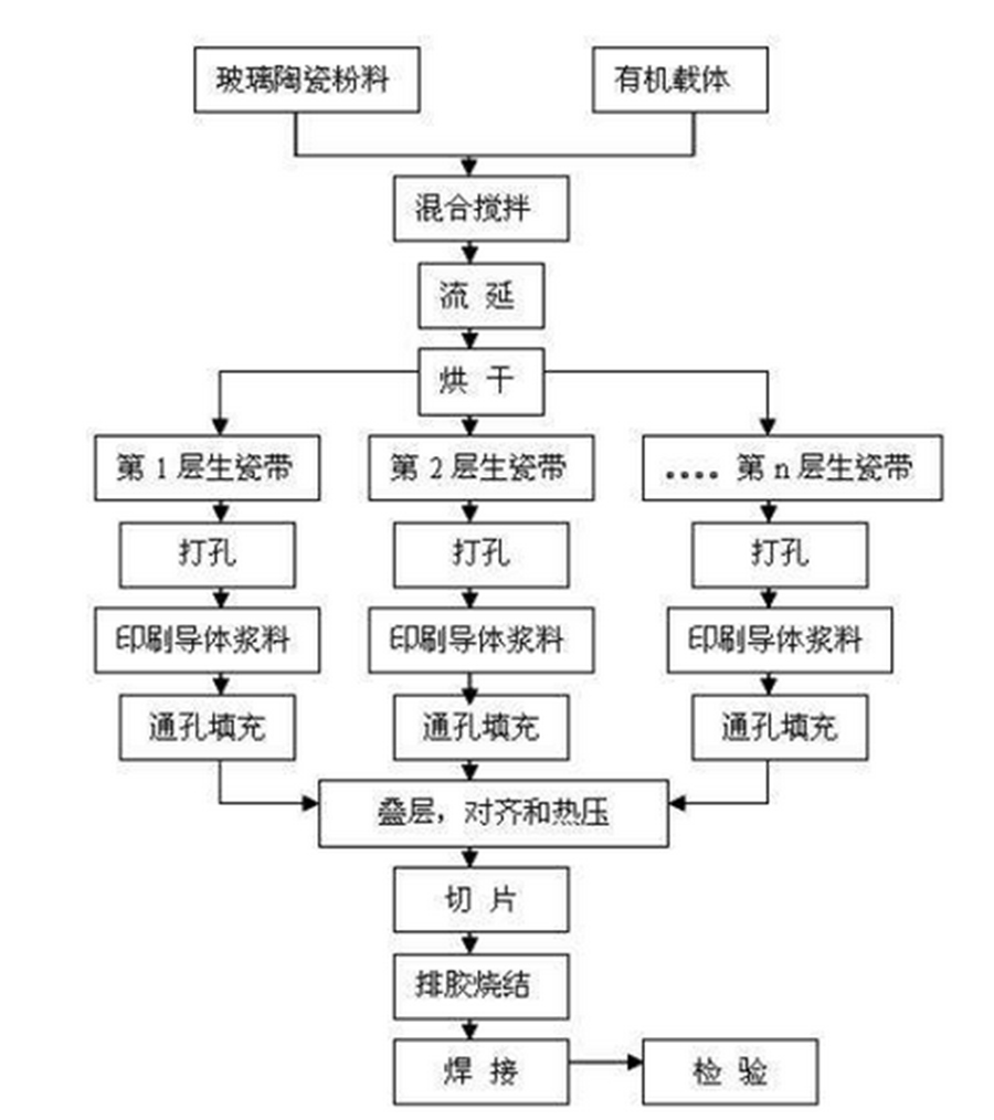
Figure 2
Mixing and casting: Organics (consisting mainly of polymer binders and plasticizers dissolved in solution) and inorganics (consisting of ceramics and glass) are mixed in certain proportions, homogenized by ball milling, and then poured onto a moving carrier belt (usually polyester film), passed through a drying area to remove all solvents, and then cast to the desired thickness by controlling the gap between the blades. Typical thickness tolerances for this process are ±6%.
Punching: Through holes are formed using mechanical punching, drilling or laser drilling techniques. Through-holes are small holes (usually 0.1-0.2mm in diameter) punched into the raw ceramic sheet for interconnecting circuits between different layers. Molded holes are also punched at this stage to aid in alignment during stacking; alignment holes are used for automatic alignment when printing conductors and dielectrics.
Printing: Conductor pastes are printed and dried using standard thick film printing techniques. Through-hole filling and conductor graphics are dried in box or chain ovens according to the relevant process temperatures and time drying. As required, all resistors, capacitors and inductors are printed and dried at this stage.
Through-hole filling: Through-holes are filled with specially formulated conductor paste with high solid particle content using conventional thick film screen printing or sample extrusion.
Degumming and sintering: The area between 200-500°C is called the organic degumming zone (it is recommended that the stack be kept warm in this zone for at least 60 minutes). The stack is then co-fired to peak temperature (typically 850°C) in 5-15 minutes. Firing of metallization typically takes 2-10 h. Fired parts are prepared for the firing process, e.g. printed conductors and precision resistors on the top surface, and then fired in air. If Cu is used for metallization, it must be sintered in an N2 chain furnace.
Inspection: The circuits are then laser-tuned (if required), tested, sliced and inspected, and leads or heat sinks can be soldered (if required) in the LTCC package.
LTCC substrate circuit processing cases
1.LTCC Substrate Microvia Formation Technology
The formation of microvias is an extremely critical process in the high-density interconnection of low-temperature co-fired ceramic multilayer substrates, as the size and positional accuracy of the vias will have a direct impact on the density of the wiring and the quality of the substrate. In order to realize ultra-high density, the through-hole aperture should be less than 100μm. The microvia production methods for LTCC tapes include mechanical punching and laser drilling.
1.1 Mechanical Punching
Punching with a CNC punch press is a better method for punching raw ceramic tapes, especially for shaped products, where punching is more advantageous. Thousands of holes can be punched out at a time with a minimum diameter of 50 μm by using a punch press mold, which is suitable for mass production due to its fast punching speed and high precision. When making micro-through holes in raw ceramic tapes, a punch of the same size as the micro-through holes and a mold are required. The opening of the mold is generally 12.5μm larger than the diameter of the punch.
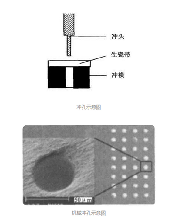
The key technical point in the production of microvias is the mounting and handling of tiny punches. Once the diameter of the punch is smaller than 100 μm, the mounting and handling of the punch becomes more and more difficult due to the reduced robustness. Most stamping defects are not formed during the stamping process, but are caused by improper handling. Therefore, special tools are needed to mount micro punches and to avoid impacts and damage to the punch during mounting and operation. Aligning the punch and die. The ability of a mechanical punch to produce a high quality through-hole depends largely on the alignment between the punch and the die. If the two devices are not aligned, the quality of the through-hole will deteriorate, the die will be damaged, and the punch may break. Ensuring the quality of microvia production, the quality of a microvia includes the shape, size and internal penetration of the microvia.
The diameter and spacing of microvias formed by mechanical punching are good. The top edge is smoother, but the bottom edge is rougher and the inner wall is straighter. The size of the top and bottom openings are similar. Different thicknesses of LTCC ceramic strips produce the same microvia size, i.e., the ratio of the thickness of the ceramic strip to the through-hole size does not affect the quality of the through-hole. The formation of 50, 75 and 100 μm microvias on different LTCC ribbons with thicknesses of 50-254 μm using mechanical punching shows that the size of the openings of the different sizes of microvias on the front and back of the LTCC ribbons are within the permissible measurement error, but that the through-hole openings on the back of the ribbons have a larger deviation. Microscopic examination of the changes in the die opening after punching showed an increase in the size of the opening compared to the original one, which was caused by wear of the die opening. The analytical data of different micro through holes show that the size of the punch determines the size of the opening on the front side of the through hole, while the diameter of the through hole on the back side is affected by the size of the die opening.
Therefore, when the die opening exceeds a certain value due to wear, the opening on the back side of the microvia will increase considerably and the die should be replaced. Another factor that affects the quality of the micro via is the residue in the via, which is a small piece of LTCC ceramic tape left in the through-hole opening that is not completely removed during punching. These residues are mainly in the back of the LTCC ceramic tape layer, connected with the edge of the through-hole, generally 10-25 μm. The number of through-holes containing residues with the increase in the size of the through-hole and reduce the amount of residue content and the thickness of the ceramic tape has nothing to do.
2.Microporous injection method
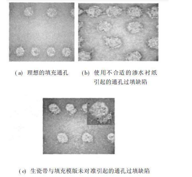
Usually the microporous injection method is the most effective, but requires specialized equipment. In the micro-hole injection system, the main factors affecting the quality of through-hole filling include injection pressure, injection time, filling paste viscosity, and alignment between the LTCC ceramic tape and through-hole filling mask. Once the parameters for the entire manufacturing process have been determined, thousands of through-holes can be filled in the LTCC bioceramic tape layer in a matter of seconds. Note the unfilled, overfilled and underfilled microvia metallization.
75μm microvias filled with silver paste. The paste-filled via has the desired size and satisfactory fill quality. Overfilled defects on the backside of the LTCC tape were caused by the use of an unsuitable porous liner between the vacuum chuck and the LTCC tape. Overfill defects occur on the front side of the LTCC tape through-hole that is in contact with the mask plate when there is misalignment between the mask plate and the LTCC tape when filling the through-hole. Top through-hole with a pitch of 75μm. The hole spacing is shortened due to overfilling. If overfilling occurs between via holes, the hole spacing must be increased to avoid short circuits caused by the additional paste from overfilling, but this will reduce the internal interconnection density.
3.LTCC substrate debinding and sintering
The technical key points of sintering are to control the sintering shrinkage rate and the overall change of the substrate, to control the sintering shrinkage performance of the two materials, to avoid micro and macro defects, as well as to realize the antioxidant effect of the conductor material and to remove the binder in the process of sintering. The sintering shrinkage of ordinary LTCC substrates is mainly achieved by controlling the particle size of the powder, the ratio of the cast binder, the pressure of the hot-pressing laminations, and the sintering curves, etc. However, the general LTCC co-firing system is not suitable for the sintering of LTCC substrates. However, the general LTCC co-firing system along the X-Y direction of the shrinkage is still 12-16%. With the help of pressureless sintering or pressure-assisted sintering techniques, it is possible to obtain materials with zero shrinkage in the X-Y direction.
Realization of zero shrinkage of the process are: self-binding sintering, the substrate in the free co-firing process to show their own inhibition of the plane direction of the shrinkage of the characteristics of this method does not require the addition of new equipment, but the material system is unique, and can not satisfy the requirements of the manufacture of different performance products. Pressure-assisted sintering, which suppresses shrinkage in the X-Y plane by sintering under pressure in the Z-axis direction; Pressure-assisted sintering, which adds an interlayer (e.g., alumina, which does not sinter at LTCC sintering temperatures) between the laminated materials to limit movement in the X- and Y-axis directions, and then grinds off the upper and lower sandwiching alumina layers after sintering; and Composite Plate Co-pressing and Sintering, in which a billet body is adhered to a metal plate (e.g., molybdenum or tungsten, etc.) for sintering, and then sintered to the plate. The composite plate co-press-firing method, in which the billet is attached to a metal plate (such as high mechanical strength molybdenum or tungsten, etc.) for sintering, utilizes the binding effect of the metal plate to reduce the shrinkage of the billet in the X-Y direction. Ceramic sheet and billet laminated co-sintering method, ceramic sheet as part of the substrate, sintered, do not have to remove, there is no inhibition of residual worries.
4.LTCC Circuit Board Large Area Ground Bonding
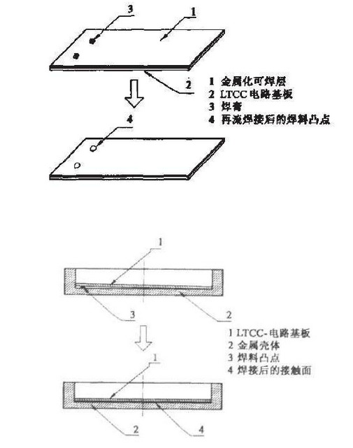
LTCC circuit board large-area grounded soldering process design to improve the LTCC circuit board large-area grounded soldering soldering rate and reliability of the soldering process. LTCC circuit board ground plane set (Ni + M) composite alloy metal film layer, according to the test test contrast, its welding resistance (> 600s) is significantly better than the conventional metallization ground layer (conventional requirements > 50s); in the LTCC circuit board ground plane is preset at one end of a “bump”, through the X-ray scanning map of the contrast analysis, increase the “bump”, the “bump”, the “bump”, the “bump”, the “bump”, the “bump”, the “bump”, the “bump”, the “bump”, the “bump”, the “bump”, the “bump” and the “bump”. Through the comparison of X-ray scanning images, the design of adding a “bump” improves the bonding rate of large-area grounded soldering. The study shows that: the new design of the soldering process ensures the reliability and consistency of the large-area grounded soldering of LTCC circuit boards.
4.1 Test materials and equipment
LTCC circuit board: the use of Ferro A6-S raw ceramic sintered into a multi-layer circuit board, size 80mm x 30mm x 1.2mm, the component shell material for the Kovar alloy, the box wall thickness of 1.0mm, the bottom size of 80mm x 30mm, the bottom of the thickness of 2.0mm, the solder for the 0.1mm-thick Sn63Pb37 solder sheet.
Test equipment: Self-made nitrogen-filled glove box with a heating table, the rated working temperature of the heating table is 450℃.
X-ray inspection equipment: MACROSCIENCE MXR-160.
Digital camera equipment: OLYMPUS MODEL NO. C5060.
4.2 LTCC circuit board surface metallization method
LTCC circuit board surface metallization method currently there are two kinds of methods: thick film sintering method and sputtering thin film electroplating thickening method. Although the sputtering thin-film re-deposition thickening method has been widely used in thin-film circuit processing of single-layer ceramic substrates, it has been widely used in LTCC circuit boards. However, it is still in the exploratory stage for LTCC circuit boards. At present, the general method to improve the solder resistance of LTCC circuit boards is to sinter a layer of palladium silver.
4.3 Solder resistance test method
Select three samples for solder resistance test comparison: (1) thick film palladium silver layer (about 12μm) sample; (2) thick film gold layer (about 37μm) sample; (3) set up with Ni Barrier layer 3 (Nj + M) composite alloy metal film (about 10μm) sample, M is the metal code.
Reference GJB548A-96 (microelectronic device test methods and programs): the substrate vertical immersion (215 ± 5) ℃ molten solder tin tank, each time 58, a total of 10 times (solder composition of 63Sn37Pb eutectic solder, flux for the 25% rosin alcohol solution) to clean, paint the solder, the examined shape should be no warpage, peeling off, fracture, be melted not more than 20% of the area. The above three samples are able to pass the test of solder resistance inspection standards, and did not see the melting of the place, and then the above three samples (new samples) metalized layer surface placed on the flux-coated pads, under nitrogen protection, 240 ℃ (set value) on the hot plate heating to maintain and observe the melting of solder corresponding to the surface of the sample metalized layer.
4.4 LTCC circuit boards and boxes of gas-shielded welding methods
LTCC circuit boards and boxes can be realized on the bottom of the large surface area of welding methods are: gas-protected welding, vacuum welding, air in the hot plate welding. When the corresponding soft solder is in liquid state in the air, it is easier to react chemically with the oxygen in the air, so gas shielded soldering has obvious advantages compared with hot plate soldering in the air. However, the two methods of gas-shielded mesh welding and vacuum mesh welding have their own advantages and disadvantages. The heat conduction in vacuum mainly relies on radiation, the shielding effect is more obvious. Due to the small size of the microwave components, the temperature on each workpiece is not uniform, resulting in high temperature of some workpieces, excessive flow of solder, and insufficient temperature of some workpieces. Incomplete melting and spreading, poor quality consistency of plasma welding, long heating cycle, low efficiency.
Gas-protected stellite welding heat conduction of the three ways to coexist, easy to operate, high efficiency, however, due to the presence of gas stellite adhesion rate is limited. In general conditions can be up to 75% or more, was randomly distributed. For microwave circuits, it brings great uncertainty. In order to increase the soldering rate, a method of pre-setting “bumps” is used. The material of the bumps is the same as that of the large-area dowel. The bump is made by placing an appropriate amount of solder paste at the corresponding position and reflowing it with hot air to form a bump. The size of the bump varies according to the length of the substrate. After the bumps are made, a solder pad of the same composition as the bumps with the oxidized skin removed is placed at the bottom of the box. A large area of ground soldering between the LTCC and the bottom of the case is realized by heating on a hot plate under gas protection.
4.5 Soldering Rate Checking
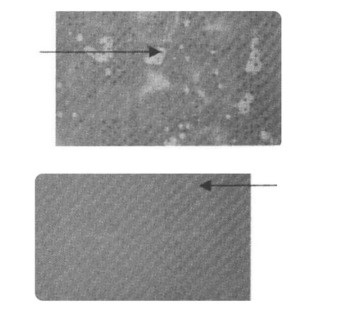
Theoretically, the solder will try to fill the gap between the LTCC and the bottom of the case as much as possible by using the principle of capillary phenomenon after large surface area soldering. However, due to the presence of protective atmosphere, the melted solder will randomly form a number of rings to enclose the gas inside. If there is a cavity inside the solder interface or if the solder alloy is loosened during solidification, the X-ray can easily pass through, resulting in white or grayish-white bright spots in the imaging image. The X-ray scan without the “bump” soldering process has arrows that indicate obvious soldering defects, with a soldering rate of about 75%, and with the “bump” soldering process. In the X-ray scan of the “bump” welding process, the arrows indicate minor welding defects with a tungsten bonding rate of 98% or more. Due to the presence of the “bump”, there is a difference in temperature between the two ends of the LTCC substrate during the heating process. As the “bump” slowly collapses, it facilitates the removal of trapped gas between the solder and the LTCC substrate at the bottom of the cassette. X-ray inspection pictures prove that the design of “bumps” on the soldering surface of the substrate can improve the soldering rate under gas protection.
4.6 LTCC circuit board large-area grounded soldering conclusion
(1) Set (Ni + M) complex alloy metal film layer, greatly improving the LTCC substrate large-area metallization layer on the Sn63Pb37 solder resistance to ensure that the LTCC substrate and the box body of the reliable soldering; (2) The use of gas protection, in the LTCC substrate soldering surface design of the “grounding soldering”; (3) The use of gas protection, in the LTCC substrate soldering surface design of the “grounding soldering”.
(2) The use of gas protection, the LTCC substrate soldering surface design “bumps” in the LTCC circuit substrate and the box between the soldering rate is very effective.
5 LTCC circuit inspection
After greasing, sintering, and soldering, LTCC components must be inspected in a variety of ways to ensure reliable performance. These tests include appearance, dimensions, strength, electrical properties, and more.