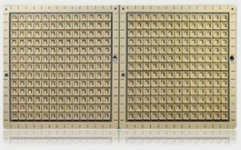
As the third-generation electronic packaging substrate technology, metal ceramic PCB is becoming the core carrier of power electronics, RF circuits and high-temperature application scenarios by organically combining the thermal conductivity of metal with the electrical insulation properties of ceramic.
The core of metal ceramic PCB lies in its unique composite structure, which is usually composed of a metal substrate, a ceramic insulation layer and a conductive copper layer. Taking the composite of aluminum nitride ceramic (AlN) and a copper substrate as an example, the thermal conductivity of aluminum nitride is as high as 170-230W/m·K, forming a gradient heat conduction channel with copper (383W/m·K), while the dielectric loss (0.001-0.1) and dielectric constant (8-10) characteristics of ceramics enable it to maintain signal integrity in the millimeter wave frequency band.
This material combination solves the three major pain points of traditional PCBs:
Thermal management bottleneck: The thermal conductivity of ordinary FR-4 substrates is only 0.3-0.4W/m·K, while metal ceramic PCBs can achieve an equivalent thermal conductivity of 10-30W/m·K, reducing the junction temperature of IGBT modules by 15-20℃.
High-frequency signal attenuation: In 28GHz 5G base station applications, the dielectric loss of ceramic substrates is 60% lower than that of traditional materials, and the signal transmission efficiency is increased by 3 times.
Environmental adaptability: The bending strength of silicon nitride ceramics (Si₃N₄) reaches 600-800MPa. Combined with the matching design of the CTE (16-18ppm/℃) of the copper substrate and the Si chip (3-4ppm/℃), the reliability of the power module is improved by 5 orders of magnitude in the wide temperature range of -55℃ to +200℃.
Manufacturing process: Precision-controlled composite technology

metal ceramic PCB
The preparation of metal ceramic PCB involves three key processes:
Direct copper bonding technology (DBC): Through eutectic reaction at 1065-1083℃, a 0.3-0.5mm copper layer is formed on the surface of alumina ceramics, with a bonding strength of more than 20MPa. This process has achieved the stable preparation of 800μm thick copper layers, meeting the high current requirements of new energy vehicle motor controllers.
Active metal brazing (AMB): Ag-Cu-Ti brazing material is used to achieve metallurgical bonding of aluminum nitride and copper substrate at 850℃, with a shear strength exceeding 35MPa, which is particularly suitable for the packaging of silicon carbide (SiC) power modules.
Laser activated metallization (LAM): Ultraviolet laser is used to excite metal nanoparticles on the ceramic surface to form a 0.1μm-level metallization layer, and the line width/spacing (L/S) resolution can reach 10μm, meeting the precision wiring requirements of high-frequency RF circuits.
Taking BYD IGBT 6.0 module as an example, the AMB ceramic substrate it uses achieves:
Thermal resistance is reduced to 0.12K/W (traditional DBC is 0.25K/W)
Power cycle life exceeds 1 million times (DBC is 300,000 times)
Module volume is reduced by 40%, and system efficiency is increased by 2%
Application scenario: Enabler of high-end manufacturing
New energy vehicle electric drive system: Tesla Model 3 Plaid's silicon carbide inverter uses aluminum nitride ceramic substrate, which reduces switching losses by 30% under the 800V high-voltage platform and increases the driving range by 5%.
5G communication base station: Huawei 64T64R AAU equipment uses low-temperature co-fired ceramic (LTCC) filters, which reduces insertion loss to 0.2dB, improves out-of-band suppression by 15dB, and expands base station coverage radius by 20%.
Aerospace field: SpaceX Starlink satellite's phased array antenna uses silicon nitride ceramic substrate, which maintains signal phase stability of ±1° in a space environment of -180℃ to +120℃, and antenna gain is increased by 3dB.
Medical laser equipment: The laser generator of Lumenis M22 superphoton instrument uses beryllium oxide ceramic substrate with thermal conductivity of 330W/m·K, which increases the pulse energy density to 50J/cm² and the treatment efficiency by 40%.
Technical challenges and development trends
Although metal ceramic PCBs have shown significant advantages, their commercialization still faces three major challenges:
Cost bottleneck: The price of aluminum nitride substrates is 8-10 times that of FR-4, mainly restricted by high-purity ceramic powder (99.6% AlN) and precision processing equipment (such as German LPKF laser drilling machine).
Process complexity: The AMB process needs to be completed in a vacuum environment, and the single-line production capacity is less than 1/3 of DBC, resulting in a delivery cycle of more than 8 weeks.
Reliability verification: In the automotive industry, ceramic substrates need to pass 1,000 temperature cycle tests from -40°C to +150°C in the AEC-Q200 standard, while the current industry yield is only about 85%.
Future technological development will focus on three major directions:
Material cost reduction: Through nano-ceramic powder modification technology, the thermal conductivity of alumina substrates is increased to 40W/m·K, and the cost is reduced to 1/3 of aluminum nitride.
Process innovation: Develop 3D printing ceramic substrate technology to achieve one-time molding of complex cavity structures, shortening the manufacturing cycle from 6 weeks to 2 weeks.
System integration: Research on the integrated packaging of ceramic substrates and embedded capacitors and resistors to reduce the module volume by 60% and reduce the parasitic inductance to below 2nH.
Metal ceramic PCBs are penetrating from high-end special applications to the mainstream market. According to Yole Développement's forecast, the global ceramic substrate market size will reach US$1.2 billion in 2025, with an annual compound growth rate of 18%. With the popularization of third-generation semiconductor devices such as silicon carbide and gallium nitride, metal ceramic PCBs will become a key enabling technology for breakthroughs in the performance of power electronic systems, promoting technological revolutions in new energy vehicles, smart grids, industrial Internet and other fields.