About CAD-aided design software and network analyser
For high-frequency circuit design,there are already good CAD software. Their powerful features are sufficient to overcome the drawbacks of design experience and cumbersome parameter retrieval calculations. Coupled with powerful network analysers, anyone with a little experience should be able to produce better quality RF components. However, this is not the case.
CAD design software relies on powerful libraries of component parameters and basic performance specifications provided by most of the world's radio equipment manufacturers.Many RF engineers mistakenly believe that as long as they use the software to design,there will be no major problems. But the actual results are always unexpected.The reason is that they give up the flexibility of applying the basic concepts of high frequency circuit board design under the wrong understanding, as well as the experience they have accumulated in applying the basic design principles.As a result, they often make basic application errors when applying software tools.

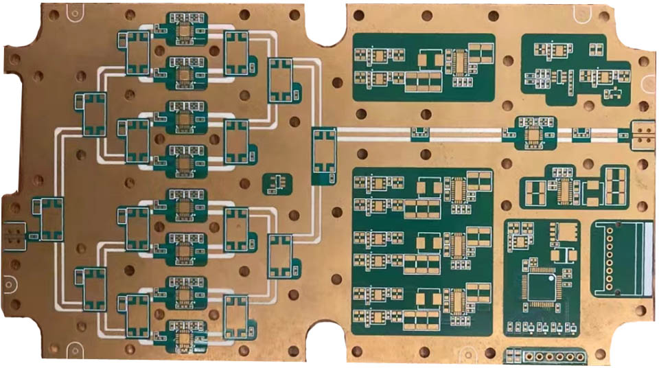
High Frequency Circuit Board
RF circuit design CAD software is a transparent visualisation software, the use of a variety of high-frequency base put aside the model library to complete the actual circuit state of the analogy. At this point,we can already understand the key aspects.There are two types of high-frequency basic configuration models, one is the component model in the form of dense parameters, and the other is the partial function model in conventional design.So there are the following problems:
(1) Component models have been developed to interact with CAD software for a long time and are becoming more sophisticated.In practice,you can basically trust the authenticity of the model. However, the application environments considered in the component models (especially the electrical environment in which the components are applied) are typical values.In most cases,it is necessary to use experience to determine a series of application parameters, otherwise, without the help of CAD software, the actual results are sometimes even farther than the design results.
(2) The conventional high-frequency base distribution models built in CAD software are usually limited to the predictability of the current application conditions and can only be confined to the basic functional model (otherwise no staff would be needed for product development and it would only be based on CAD to do all this. Product).
(3) It is particularly noteworthy that the typical functional model is built up through typical component applications,typical complete process methods (including PCB construction), and its performance is also at a ‘high level’.
But in reality, it is a complete imitation, and the model state is far from.The reason for this is that although the selected pcb components and their parameters are the same, their combined power environment is not. In low-frequency or digital circuits, this small difference is not a big obstacle,but in RF circuits, fatal errors often occur.
There are two types of network analysers: scalar and vector, which are essential for RF circuit design.It is common practice to combine basic RF circuit design concepts and principles to complete the circuit and PCB design (or use CAD software to do so), complete the PCB prototyping and assembly of samples as required, and then use a network analyser to design each link.Only through network analysis can the circuit be optimised.
However, the price of this work is the actual production of at least 3 to 5 versions of the PCB. without the basic principles of PCB design and basic concepts, more versions of the PCB will be required (or not be able to complete the design).
As can be seen from the above:
(1) in the process of using the network analyser to analyse the RF circuit,there must be a complete high-frequency circuit PCB design concepts and principles, and must be able to analyse the results of the PCB design defects clearly know. Only this item requires relevant engineers.Have considerable experience.
(2) in the process of analysing the prototype network links,must rely on skilled experimental experience and skills to construct a local functional network. This is because in many cases, circuit defects found by network analyzers can have multiple causes at the same time,so the construction of local functional networks is needed to analyze and thoroughly identify the causes.
The construction of such high-frequency circuits must rely on clear RF circuit design experience and skilled circuit PCB construction principles.