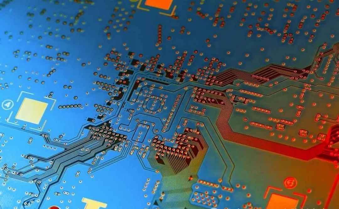
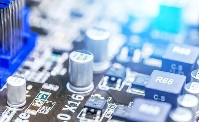
Mobile Phones PCB,which stands for Printed Circuit Board, is one of the most critical components inside a mobile phone, responsible for power,signal transmission,and interconnecting different modules.The distribution of layers on a PCB is crucial, and now let's delve into the details.
Typically,mobile phones PCB adopts either a four-layer or six-layer design.The four-layer PCB has a relatively simple layer distribution, consisting of two main layers:the top layer and the bottom layer. The top layer houses the main chips, signal lines,and components like the keypad,while the bottom layer is primarily used to connect the battery, power supply,and other modules. Four-layer PCBs were commonly used in early mobile phones but have largely been replaced by six-layer PCBs today.
The six-layer PCB has a more complex distribution.In addition to the top and bottom layers,there are four internal layers,which are primarily used to connect chips, signal transmission, the display, and other modules.The top and bottom layers mainly accommodate critical modules such as signal connections,power,and components like the camera,accessory interfaces,etc.The internal layers house components such as the processor,memory,wireless modules, and other electronic parts.

The layer distribution of mobile phone PCB has a critical impact on the overall performance of the phone. Specifically, the PCB layout determines how various electronic components inside the phone connect and collaborate, directly affecting signal transmission quality, operational efficiency, and battery energy consumption. The stability and speed of signal transmission are often closely tied to PCB design, especially in the layout of wireless communication modules, Wi-Fi, Bluetooth, GPS, etc. A well-designed layer distribution helps minimize signal interference and loss, enhancing data transmission speed and accuracy.
Moreover, the structure and layout of the PCB also determine the efficiency of internal space utilization in the mobile phone. With the continuous increase in the functions of smartphones, internal space becomes increasingly constrained, making it a significant challenge for designers to place more functional modules in a limited space. By optimizing the layer distribution, designers can maximize the phone's integration while ensuring the functionality remains operational without compromising thermal performance.
The phone's battery consumption is also a crucial factor influencing user experience. A well-designed PCB can optimize the power management system and reduce energy waste, thereby extending battery life. For example, efficient power transmission paths and well-positioned power layers can maintain high performance while minimizing power loss, improving battery endurance.

With the rapid development of smartphone technology,mobile phone PCB design and manufacturing processes are constantly improving. From early single-layer and double-layer PCBs to today's multi-layer, high-density PCBs, there are increasing demands for higher electrical performance and more refined mechanical designs. Multi-layer PCBs enable smartphones to integrate more circuits and functions within a limited volume, while also improving electrical performance and stability. Especially with the advent of 5G technology, AI processors, and more complex sensors and display technologies, mobile PCB design must meet higher frequencies, greater data transmission demands, and stricter thermal management requirements.
Additionally, in mobile PCB design, designers establish specific routing and interconnection principles based on layer distribution to enhance the communication between modules, as well as the sending and receiving of signals to and from the external environment. In conclusion, the layer distribution of mobile phone PCB plays a crucial role in signal transmission,operational efficiency, and power consumption. As mobile technology continues to evolve, the structure and distribution patterns of PCBs are also continually optimized and improved.