The planning of PCB board is very important for the anti-disturbance of microcontroller system. To control the source of noise as far as possible, as far as possible to reduce the propagation of noise and coupling, as far as possible to reduce the absorption of these three principles of planning PCB boards and wiring.
1.PCB board to a reasonable partition, the MCU system can generally be divided into three areas, namely, the imitation circuit area (fear of disturbance), digital circuit area (anti-stirring, but also stirring), the power drive area (source of disturbance).
2.PCB single point grounding principle of power supply. Three areas of the power line, ground from the point of the three-way lead, noise components and non-noise components should be far away from some.
3.Clock oscillator circuit, especially high-speed logic circuit part of the ground looped up, so that the circumferential electric field close to zero.
4.I / O driver equipment, power amplifier equipment as close as possible to the edge of the PCB board, close to the lead out of the plug-in programme.
5.Can use the clock to satisfy the minimum required frequency of the system, the clock generator should be as close as possible to the equipment used for the clock.

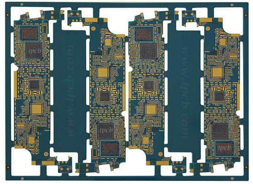
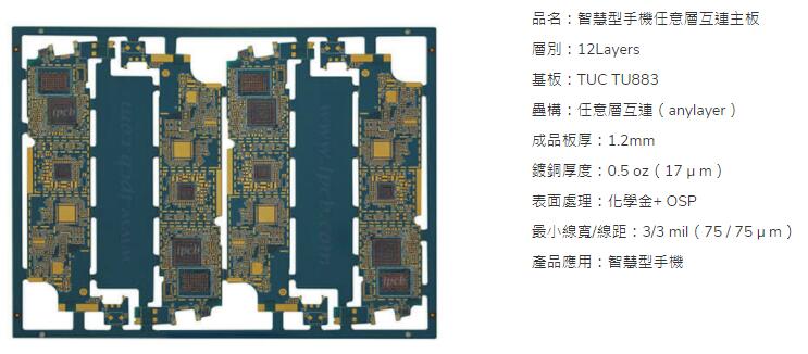
Mobile Phone PCB
6.The quartz crystal oscillator case should be grounded, and the clock wire should be as short as possible and not lead all over the place.
7.Use a 45-degree bend in the wiring, not a 90-degree bend, to minimize the emission of audio signals.
8.Single-panel, double-panel, power line, ground line should be as thick as possible, the signal line of the hole should be as few as possible.
9.4-layer board than dual-panel noise 20dB lower than 6-layer board than 4-layer board noise 10dB lower than the economic conditions allow as much as possible with multi-layer board.
10.The key line as short as possible and to be thick, and on both sides of the protective ground, the sensitive signal and noise field band signals through a flat-band cable out of the case, to use the ground - signal - ground pipeline out.
11.Do not form a loop underneath the quartz oscillator. If this is unavoidable, the loop should be as small as possible.
12.Clock lines perpendicular to the I/O lines are less disturbing than those parallel to the I/O lines, so keep the clock lines away from the I/O lines.
13.For A/D equipment. The digital part can be wrapped around and do not cross, noise-sensitive lines do not and high-speed lines. High current parallel.
14.Microcontroller and other IC circuits, such as multiple power. If there are multiple power and ground terminals, add a decoupling capacitor at each end.
15.Each IC to have a decoupling capacitor, to choose a good signal for the decoupling capacitor. When the decoupling capacitor is soldered on the PCB, the pins should be as short as possible.
16.The signal from the high noise area should be filtered, and a discharge diode should be added at the relay coil. Can use a negative method to soften the IO line jumping edge or provide a certain amount of damping.
17.Use long-capacity tantalum or polyester capacitors instead of electrolytic capacitors as energy storage capacitors for circuit charging.Because electrolytic capacitors have a large inductance distribution and are ineffective at high frequencies, electrolytic capacitors should be used in pairs with good decoupling capacitors with high special effects.
18.When required, the power cord. Ground can be added to the copper wire wound ferrite and become a high-frequency choking equipment to block the transmission of high-frequency noise.
19.Weak signal lead wires, high-frequency, high-power lead wires to be added to the mask, lead wires and ground wires to be twisted up.
20.The PCB board is too large or the frequency of the signal line is too high, so that the delay time on the line is greater than or equal to the signal rise time,the line should be processed according to the transmission line, to add the terminal matching resistor.
21.Don't use IC sockets as much as possible, solder ICs directly on the PCB, IC holders have a larger capacitance spread.

Mobile Phone PCB
Decoupling Capacitor
Each IC should be equipped with a decoupling capacitor between the power supply and ground,which can filter out high-frequency noise from the power supply.As an energy storage element, it absorbs or provides IC internal triode conduction, cut-off caused by current changes, and then reduce system noise.To choose a high frequency effective monolithic capacitor or ceramic capacitor with a winding structure,its distribution inductance is larger, and it is almost ineffective in filtering out high frequency signals, and it should be used in pairs with decoupling capacitors when it is effective. Tantalum capacitors are better than electrolytic capacitors.
Suppressing high-frequency inductance
High-frequency inductance suppression equipment is constructed by threading thick enameled wire into a ferrite core with several axial holes. It can be tampered into the power line or ground line to block high frequency signals from being introduced into the power/ground line.This component is particularly suitable for separating the analog and digital circuit areas on a PCB and for powering high power drives. It should be noted that it must be placed in the area between the storage capacitor and the power supply,and can not be placed between the storage capacitor and the appliance.
Fourth, low noise series of microcontroller
Traditional IC planning,in the power supply, ground on the lead-out will generally be arranged on both sides of the symmetry, such as the lower left corner is the ground, the lower right corner is the power supply, which makes the power supply noise through the entire silicon. Improved skills will be arranged in the power supply, ground on two adjacent pins, which on the one hand reduces the flow through the entire silicon, on the one hand, so that the external decoupling capacitors in the PCB board planning is more simple to arrange in order to reduce the system noise.Another IC planning to reduce noise, such as the driver circuit planning. Some microcontrollers provide a number of output pins with high currents, ranging from a few milliamperes to hundreds of milliamperes.The integration of these high power driver circuits into the microcontroller undoubtedly adds a new source of noise. This can be eliminated by a softening technique along the jumping edge. The method is to make a high-power tube into a number of small tubes in parallel, and then the output of each tube string of different equivalent resistance resistors to reduce the noise source.