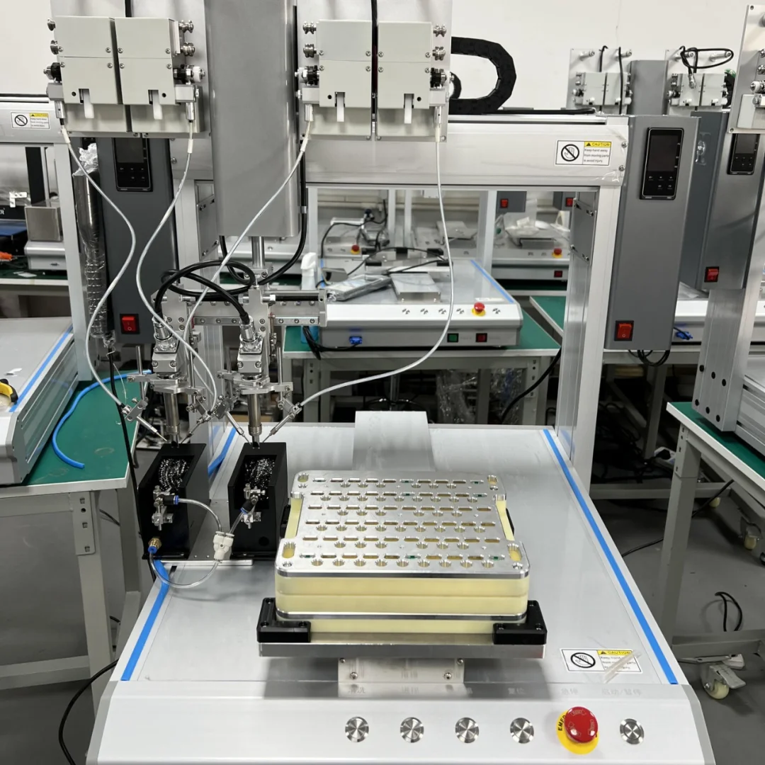
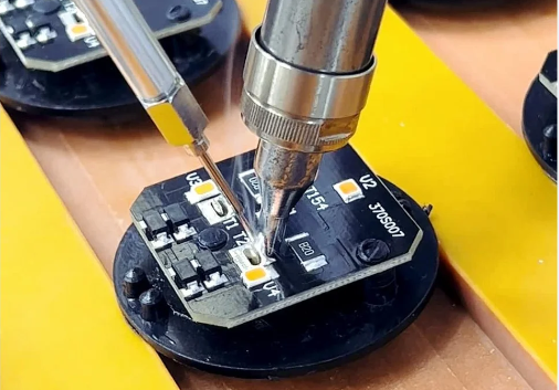
Motherboard soldering is a critical process in electronic manufacturing, primarily used to secure components to the printed circuit board (PCB). Solder is a low-melting-point metal alloy, typically composed of tin, lead, or other metals. During soldering, heat is applied to melt the solder, allowing it to connect component leads with the PCB's pads or vias, forming both mechanical and electrical connections.
I.Motherboard Soldering Process and Technical Requirements
Before soldering, the PCB and the electronic components to be soldered must be prepared. Component leads are typically inserted into the PCB's through-holes or placed directly onto surface-mount pads. During soldering, tools such as soldering irons or other heating equipment are used to heat the solder to its melting point.The molten solder flows and fills the gap between the component leads and pads, creating a strong electrical connection.
Temperature control during soldering is critical. Excessive temperature or prolonged heating can damage components or the PCB,while insufficient heat may result in weak joints, leading to cold solder joints or dry joints that compromise the motherboard's long-term reliability. Therefore, precise temperature management and timing are key to ensuring solder joint quality.
Lead-Free Solder and Environmental Requirements
In modern electronic manufacturing, driven by environmental regulations, lead-free solder has largely replaced traditional lead-based solder. Lead-free solder typically consists of tin-copper or tin-silver-copper alloys. While these alloys have higher melting points, they are less harmful to the environment and human health. However, the higher melting point of lead-free solder also demands more advanced equipment and skills from operators.
II. Soldering Quality and Automated Soldering Technology
The quality of soldering directly impacts motherboard performance and lifespan. Defective solder joints, such as cold solder joints, dry joints, or cracks, can lead to short circuits, open circuits, or even complete motherboard failure. To enhance precision and consistency, modern factories often use automated soldering equipment such as reflow soldering and wave soldering.
Reflow soldering: Used in surface-mount technology (SMT), reflow soldering uses hot air or infrared heat to melt the solder paste, forming solid and reliable solder joints.
Wave soldering: Suitable for through-hole technology (THT), wave soldering involves passing the PCB over a wave of molten solder, creating connections between component leads and pads.
III. Comparison Between Fully Automated and Semi-Automated Soldering
(1) Fully Automated Soldering: The entire soldering process is completed by machines, suitable for high-volume production. Its advantages include efficiency, stability, and fewer errors, but it involves high equipment costs, making it ideal for high-precision, large-scale production.
(2) Semi-Automated Soldering: Operators participate in parts of the process, such as adjusting soldering parameters or controlling electrode positioning. This approach is suitable for small-to-medium batch production or applications requiring flexibility, where soldering parameters can be adjusted based on product requirements. However, the process is relatively less efficient.

Automatic Soldering
IV. Three Types of Automatic Soldering Methods
(1)Compression Soldering: Used for products where the solder points are evenly distributed and have specific tensile strength requirements. It is ideal for products without through-hole components, ensuring robust solder joints and high tensile strength.
(2)Drag Soldering: Suitable for products with evenly distributed solder points where the distance between solder points exceeds 0.1mm. This method is commonly used for products requiring fixed through-hole components, but if the spacing is less than 0.1mm, bridging can occur. Wave soldering or reflow soldering are faster alternatives in such cases. Drag soldering improves efficiency by saving time.
(3)Point Soldering: This method is used for products with unevenly distributed solder points or where the solder points require high saturation levels. It is also suitable when certain solder points need to be fixed before applying solder. Point soldering ensures high precision and is commonly used for electronic chip soldering.
V.Common Soldering Defects and Detection Methods
(1) Solder balls:Small solder spheres that form around component leads, potentially causing short circuits.
(2) Cracked solder joints:Small cracks in the solder joints or at the junction with the pad, which may lead to failure under vibration or temperature changes.
(3) Lifted pads:The separation of pads from the PCB, typically due to thermal stress or poor soldering techniques.
(4) Solder bridging: Solder connects adjacent solder points, causing short circuits.
(5) Old solder joints or dry joints: Incomplete solder flow or the presence of air bubbles, reducing electrical performance.

VI.Soldering Quality Detection Methods
(1) Visual Inspection: Checking the solder joints' appearance for defects such as cold solder joints, uneven soldering, or inadequate coverage.
(2) X-ray Inspection: Used to examine the internal structure of solder joints, checking for voids or solder density issues.
(3) Ultrasonic Testing: Utilizes high-frequency vibrations to detect cracks or voids in solder joints.
(4) Optical Inspection: Automated optical inspection (AOI) systems are used to detect surface defects such as oxidation or contamination.
(5) Electrical Performance Testing: Evaluates the soldered area's resistance, capacitance, and inductance to assess solder joint quality.
(6) Thermal Shock Testing: Simulates extreme temperature variations to assess the solder joints' reliability and stability under stress.
VII.The Role of Soldering Materials
(1) Sponge:Used to clean soldering tools (such as soldering iron tips) to remove old solder and contaminants.
(2) Rosin:Acts as a flux, helping the solder flow more smoothly and adhere better by reducing oxidation on the metal surface.
(3) Solder Paste:A mixture of tiny solder particles and flux used in SMT processes to temporarily hold components on the PCB before reflow soldering,forming both electrical and mechanical connections.
VIII. Preventing Soldering Defects
(1) Optimizing Pad Design:Avoid using vias within pads to prevent solder leakage and ensure sufficient solder material.
(2) Maintaining Clean PCB Surfaces:Removing oxidation layers or contaminants improves solderability.
(3) Ensuring Adequate Solder Paste:Regularly replenishing solder paste ensures enough material for robust joints, preventing cold solder joints.
By employing proper soldering techniques,leveraging automation, and utilizing advanced inspection tools,manufacturers can ensure high-quality solder joints,thereby enhancing the performance and reliability of electronic devices.