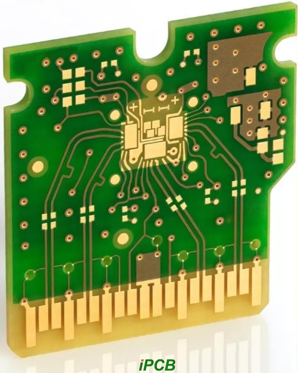
Optical module circuit boards, also called optical module PCBs, are circuit boards used in optical fiber communication devices.With the increasing demand for massive parallel data computation in AI large-scale model training and inference, the world is facing greater demands for network bandwidth, driving the accelerated iteration of optical modules and promoting the rapid development of new technologies such as CPO, LPO, and silicon photonics. Optical module PCBs are mainly used in high-speed communication fields such as optical fiber modules, 5G, and large data centers.
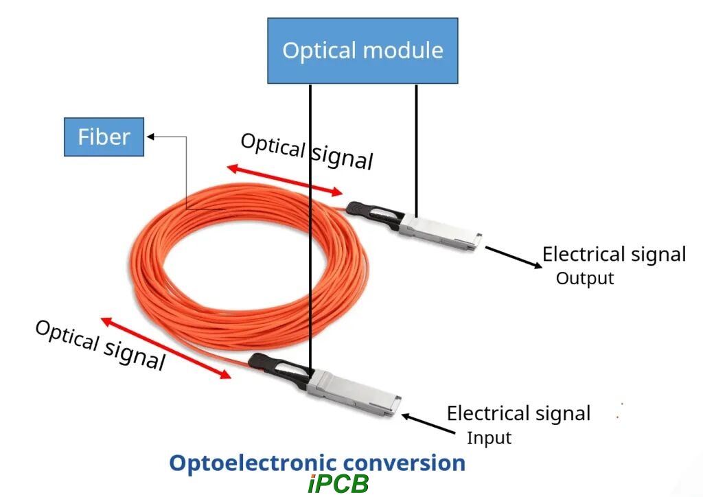
Optical modules are assembled from optical chips and optical devices and then inserted or embedded into optical communication equipment for external connections. In optical fiber communication, they are used for the mutual conversion between electrical and optical signals, performing electro-optical conversion at the transmitting end and optical-electrical conversion at the receiving end.
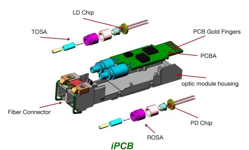
Optical module PCB composition: mainly includes four key parts: PCBA (Printed Circuit Board Assembly), TOSA (Optical Transmitter Submodule), ROSA (Optical Receiver Submodule), and the housing.
• PCBA: Printed Circuit Board Assembly
• TOSA: Transmitting Optical Sub-Assembley
• ROSA: Resceiving Optical Sub-Assembley
With the demands of low power consumption and high bandwidth in the computing era, the technical requirements for optical module PCBs are mainly determined by:
• Optical module packaging
• Optical module transmission rate
• Special application requirements of optical modules, such as heat dissipation, hot-swappable connectors, and applications in various industrial environments.
Key Technical Requirements for optical Module PCBs
1. Line Capabilities
• Line Width/Space: From traditional 100/100um, tolerance +/-20um, to 30/30um, tolerance +/-10um, and even finer lines and tolerances.
• Impedance Tolerance: From traditional impedance tolerance +/-10%, to +/-7%, and even +/-5%.
2. Alignment Capability
• Laser Via/Pad Diameter: From traditional 100/250um, to 75/130um, and even 50/110um.
• Solder Mask Ink Accuracy: Solder mask window and pad alignment accuracy from traditional +/-25um to +/-15um, or even smaller.
• Shape Accuracy
Shape Tolerance: +/-0.1mm.
Hole Center-to-Hole Center Tolerance: From traditional +/-0.075mm to +/-0.038mm.
Pad Center-to-Pad Center Tolerance: From traditional +/-0.075mm to +/-0.05mm.
PCB Board Edge to Gold Finger Tolerance: +/-0.05mm.
Slot Diameter Tolerance: +/-0.05mm.
Slot to Gold Finger Tolerance: +/-0.1mm.
3. Wire Bonding
• Wire bonding pad size 90/90um, dimensional tolerance +/-15um.
• Wire bonding pull force >= 5g, ball shear test required.
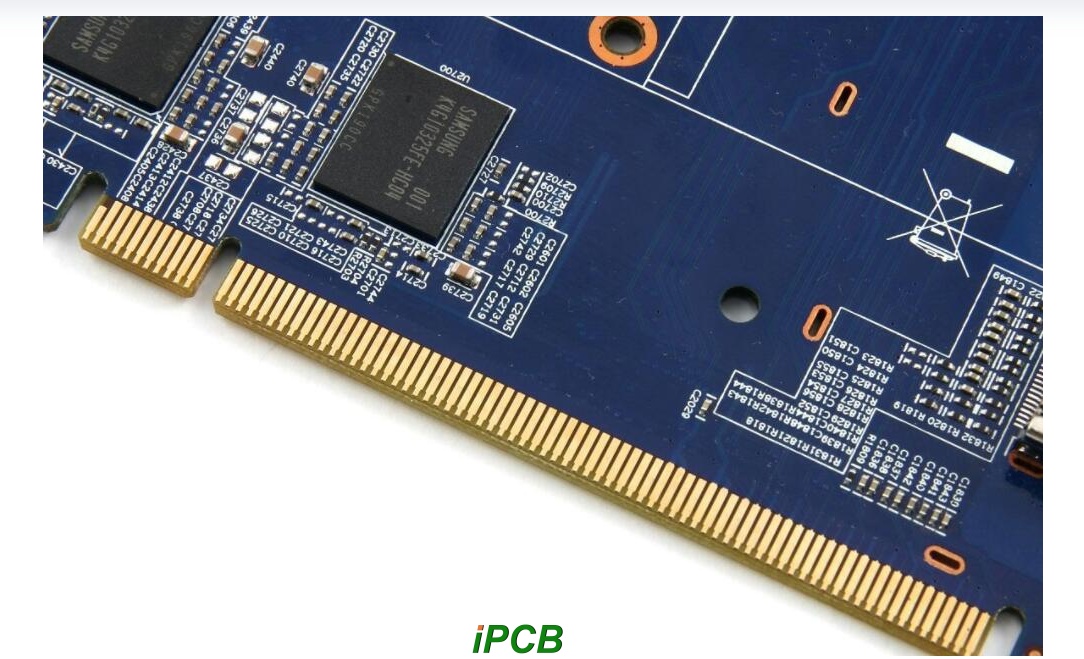
4. Gold Fingers
• Strict appearance requirements, such as no exposed nickel, no bumps, dirt, scratches, etc., specific requirements depend on customer specifications.
• Corrosion resistance: Must pass customer-specified tests, such as MFG testing, etc.
• Insertion and extraction resistance: Must pass customer-specified insertion and extraction tests, such as >= 500 insertion and extraction cycles.
• Hot-swap capability: Graded/segmented gold fingers, no lead wire residue, and meets customer quality requirements.
• Board thickness in gold finger area: Relatively strict tolerances, must meet customer requirements.
5. Embedded Copper Block
• Embedded Copper Block Flatness: 0~-10um
Core Characteristics of Optical Module PCBs
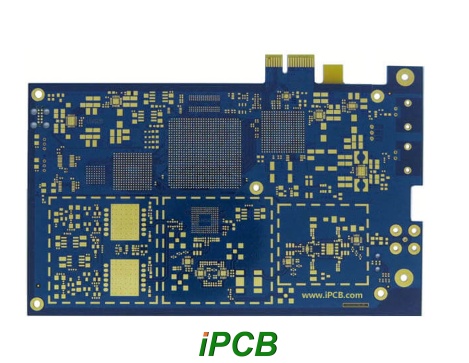
Compared to ordinary PCBs, optical module PCBs have the following significant characteristics, which directly determine their manufacturing difficulty and cost:
1. High Frequency and High Speed: Transmission rates have evolved from the early 1G/10G to the current 400G/800G and even 1.6T, requiring PCB materials with extremely low dielectric constants Dk and dielectric loss factors Df to reduce signal loss and distortion during transmission.
2. High-Density Interconnect (HDI): The miniaturization of optical modules (e.g., SFP, QSFP-DD) requires the integration of multiple chips such as TIA, LDD, MCU, and CDR. With extremely limited wiring space, HDI technology must be used, such as blind/buried vias, microvias, and VIPPO.
3. Hybrid Material Design: To balance performance and cost, hybrid voltage structures are often used. For example:
• RF signal lines: Use expensive high-speed boards (such as Rogers series, Panasonic Megtron series, Taconic, etc.).
• Power and control lines: Use lower-cost FR-4 boards.
4. High-precision impedance control: High-speed differential signals (such as 100Ω differential pairs) have extremely stringent requirements for impedance consistency, typically requiring tolerances within ±10% or even ±5%. This places extremely high demands on linewidth, dielectric thickness, and etching uniformity.
5. Good thermal management: Components such as lasers (LDs) and drivers within the optical module generate heat. The PCB needs excellent heat dissipation performance, sometimes employing thick copper foil, metal substrates (such as aluminum substrates), or through-hole designs.
Optical Module Transmission Distance
Optical module transmission distances are categorized into short-distance, medium-distance, and long-distance. Generally, distances of 2 km or less are considered short-distance, and 30 km or more are considered long-distance.
In practical applications, the transmission distance of optical modules is limited, primarily due to signal loss and dispersion during transmission within optical fibers.
Loss refers to the gradual weakening of optical signal intensity as it propagates through the optical fiber medium. It is measured in dB/km.
The main sources of optical signal loss include absorption loss, scattering loss, bending loss, and connector/joint loss in the fiber material. Generally, single-mode fiber has lower loss than multimode fiber.
Dispersion refers to the phenomenon where different frequencies or modes of optical signals propagate at different speeds within the optical fiber, causing pulse broadening and resulting in signal distortion. It is measured in ps/(nm•km).
Dispersion causes adjacent pulses to overlap, increasing the bit error rate and limiting the maximum transmission rate and unrepeater-free transmission distance of the optical fiber.
Optical Module Transmission Modes
Based on the transmission mode of the optical signal in the fiber, optical fibers can be classified as single-mode fiber (SMF) and multimode fiber (MMF). To accommodate different types of optical fibers, optical modules are also categorized as single-mode and multimode.
• Single-mode optical modules: Single-mode optical modules are used with single-mode optical fibers. Single-mode fibers have a thinner core and transmit signals using a single mode of light. This results in less dispersion during transmission and a larger transmission capacity, making them suitable for long-distance transmission.
• Multimode optical modules: Multimode optical modules are used with multimode optical fibers. Multimode fibers have a thicker core and transmit signals using multiple different modes of light. This results in greater dispersion during transmission, leading to lower transmission performance compared to single-mode fibers. However, they are less expensive and suitable for smaller capacity, short-distance transmission.
Optical module PCBs, as the core component of optical modules, must be able to operate stably in harsh industrial environments such as high temperature, high humidity, and strong electromagnetic interference. Furthermore, customized design and production are required for the specific needs of different industrial scenarios. iPCB is committed to providing high-quality, customized PCB solutions for the optical module field, meeting the application needs of various complex industrial environments and helping customers gain a greater advantage in the fierce market competition.