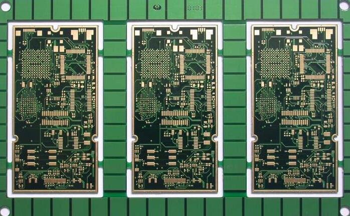
Panel circuit boards, also known as PCB arrays. Panel circuit boards are essential when considering the utilization of PCBs. The process of assembling multiple PCBs onto one large board for manufacturing is called panel circuit boards. PCB panel circuit boards are a manufacturing technology that integrates smaller PCB boards together to form an array, making it easier to pass through the assembly line. And it is also very easy to separate or remove each PCB board from the array for easy packaging or installation into the product. Or, the width is increased by setting PCB processing edges around a single PCB to accommodate the assembly line.
Panel circuit boards are often used for high-volume PCB production. panel circuit boards not only increase total output, but also allow designers to adjust the size, thereby increasing the overall utilization of PCB boards and saving costs. In the process of placing PCB orders, there are always different types of circuit boards to choose from: single board design or panel circuit board design. Because some circuit boards are irregular, panel circuit boards can reduce the time cost and labor cost of production and testing. If the PCB size is too large to pass the panel circuit board or there are other special requirements, additional planning is required.
PCB manufacturers will help customers connect single circuit boards (same or different) to large panels through different wiring processes, and the reserved micro-grooves can easily split them into individual PCBs when you need them. There are usually three types of wiring processes: V-shaped scribing, Tab wiring, and punching.

Advantages of creating PCB panels.
PCB panel circuit boards: help improve production efficiency and safety
Large-scale production: multiple circuit boards can be produced at the same time, saving time and reducing costs.
Product safety: The circuit boards are shock-proof and pressure-proof, thus ensuring the long life and normal operation of the product.
Speed and efficiency: make steps such as printing paste, assembly, connection, and testing simpler
Standard size of the panel: a recommendation for cost reduction, usually 18 inches x 24 inches
Reduce costs: reduce production costs by optimizing the amount of material used to reduce waste.
Improve efficiency: reduce changes in production, thereby providing better product reliability and quality.
Easy assembly: the assembly process is accelerated because it becomes easy to handle and organize multiple circuit boards.
Considerations when designing a tab-routed panel
For PCB assemblies that are close to the edge and non-rectangular, tab-routed panelization is preferred, but care must be taken to select a design for strength and functionality to maintain compatibility with the breakout process.
Clearance: Tabs should be spaced at least 1/8" from components and traces to avoid tension that could cause the board to break. If surface mount multilayer ceramic chip capacitors are used, they should be spaced at least 1/14" apart.
Knockout: Any holes larger than 0.6" in the design will need to be knocked out, and may need to be punched there until it is soldered. They are especially important in the middle of the array.
Tab Location: Place tabs approximately every 2 to 3" along the edge of the board, and every 1.5", placed at the edge but not under overhanging components.
Punch Location: The punch holes will be at the edge of the PCB, or for 2 PCBs, on either side of the tab.
Array Arrangement: All tabs should be pre-cut along consistent lines to prevent tearing of the laminate.
When is a panel circuit board necessary?
In many cases,panel circuit boards must be considered to improve manufacturing efficiency, reduce product costs, and quality control. Here are some examples of when PCB panel circuit boards are used:
1. Mass production--without it, mass production is impossible; many PCBs need to be processed at the same time.
2. Manufacturing efficiency--improve manufacturing efficiency, reduce costs, and simplify production processes.
3. Standardization--standardize the installation and use of any equipment and manufacturing tools that work with PCBs, thereby reducing material waste and setup time.
4. Protection during processing--protect individual PCBs from damage during processing and assembly.
5. Reduce costs--carriers promote consistency and quality control by applying constant processing conditions to various PCBs.
6. Cost-effective--maintaining high power efficiency makes it economically feasible to replicate small PCBs on panels.
7. Complex design-improve production comfort, increase manufacturing yields, and meet SMT fixture requirements.
In the field of electronic manufacturing, panel circuit boards are a key link! Integrating multiple PCB designs into the same panel can not only significantly reduce costs, but also significantly improve production efficiency and ensure consistent quality of various products. However, to truly leverage the advantages of PCB panel circuit boards, it is essential to master core technologies such as V-scribing, lug routing, strictly follow design rules, and promptly resolve potential problems at an early stage - all of which requires careful planning and precise execution.
Keeping up with new developments in panel circuit board technology and processes is a way to stay competitive in the evolving electronics market. Adopting this best approach with creative solutions can provide better results and gain a competitive advantage in the market. With deep industry accumulation and cutting-edge technology reserves, iPCB is well versed in the essence of PCB panel circuit boards. We have an experienced team of professionals who can tailor panel circuit board solutions for you, from design optimization to process control, every detail is refined.