A Trustworthy PCB and Electronic Manufacturing Enterprise! Contact Us


Under 10 times magnification, 0402 package resistance solder joints show a perfect half-moon shape, which is the production line process parameters adjusted 37 times after the results. pcb board assembly, details like this control, is reshaping the quality standards of modern electronics manufacturing - PCBA (Printed Circuit Board Assembly) as the “nerve center” of electronic products, its manufacturing precision has entered the micron-level competition era.
Solder paste as the PCBA “blood”, the proportion of its composition directly affects the welding quality. A military unit used SAC305 solder paste (Sn96.5% / Ag3.0% / Cu0.5%), under nitrogen protection can be realized under the solder IMC layer thickness of 1.5-3μm of the ideal value. The Sn63/Pb37 solder paste commonly used in consumer electronics is still irreplaceable in certain high-temperature scenarios due to its liquid-phase line temperature of 183℃.
Temperature profile requirements for reflow soldering in a typical 8 temperature zone:
Preheat zone: 1.5°C/s ramp up to 150°C to activate fluxes
Equalization zone: 90 seconds at 180-200°C to eliminate component temperature differences
Reflow zone: peak temperature 245 ± 5 ℃, duration of 40-60 seconds
Cooling zone: >3°C/s cooling rate to prevent whisker growth

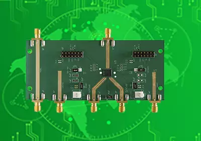
A 5G base station amplifier board layout optimization case shows that after adjusting the RF device position, the signal loss is reduced by 0.7dB@28GHz.
High-frequency devices need to be >3mm from the board edge to prevent signal reflection.
The distance between electrolytic capacitors and heat generating components should be >5mm.
BGA chip diagonal positioning holes need to be set, accuracy ±0.05mm
1. Details of the chip placement process
(1) hole size = pad area × (0.8-1.1), QFN devices need to do 10 ° tapered openings
(2) 0.12mm thick stencil suitable for 0.4mm pitch BGA, demolding speed control at 10mm/s. A cell phone main (3) board production line by reducing the stencil opening by 5%, successfully solved the 01005 component monument problem.
(4) High-speed machine mounting speed up to 85,000CPH, but 0402 components below the recommended medium-speed machine.
(5) The vacuum value of the suction nozzle needs to be maintained at -75kPa ± 5%, regularly test the mounting pressure with a piece of glass.
(6) The comparative data of an industrial control board manufacturer shows that after switching to ceramic suction nozzles, the throw rate is reduced from 0.3% to 0.07%.
(7) Oxygen content control at<1000ppm can reduce oxidation
(8) Speed deviation ± 0.1m/min will lead to peak temperature fluctuations of 8 ℃. A LED driver power supply due to chain speed fluctuations lead to false soldering, after the addition of servo motors to reduce the defective rate of 80%.
2. Finished product inspection pcb board assembly
(1) the gold standard of visual inspection
Solder joint gloss: the new tin surface should show a mirror reflection, oxidation is foggy
Component offset: chip component end exposed pad<1/4, QFP pin offset <0.1mm
An automotive electronics factory developed a 200-page visual inspection manual to compress the misjudgment rate from 15% to 3%.
(2) Algorithm revolution of AOI
Inspection accuracy increased from 0.1mm to 0.01mm in early days
Adopting multi-spectral imaging technology to recognize tin whiskers of 0.02mm
After the introduction of 3D AOI to a server motherboard production line, the detection rate was increased from 92% to 99.5%.
(3) X-RAY's Perspective Eye
When detecting BGA solder balls, the tube voltage needs to be adjusted to above 90kV.
Void rate standard: automotive electronics<5%, military industry <3
A medical equipment manufacturer successfully captured 0.15mm micro-cracks by adjusting the X-ray tilt angle.
(4) The Ultimate Trial of Functional Testing pcb board assembly
ICT test coverage needs to be >95%, boundary-scan to solve BGA test problems
Aging process: 85°C high-temperature loaded operation for 72 hours
Test data from a PV inverter manufacturer shows that 72 hours of aging screened out early failures by 0.8%.