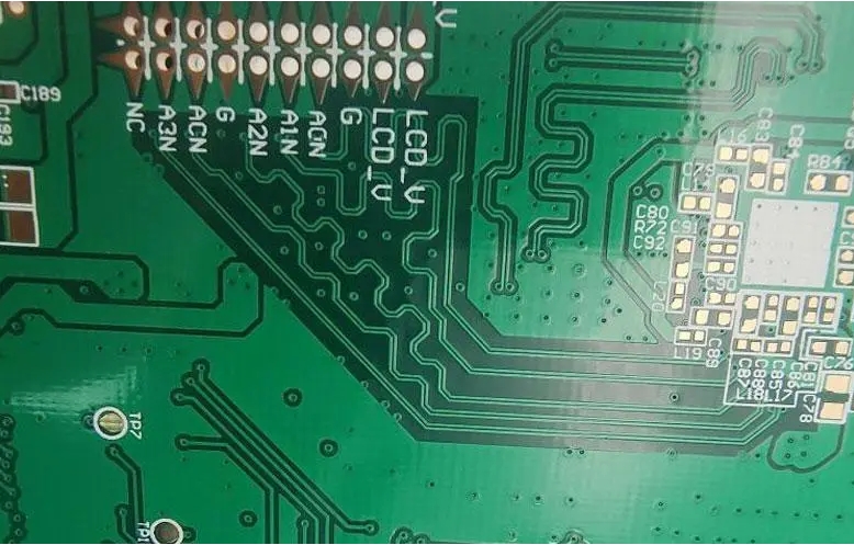
PCB boards are often delaminated during use.
Reason:
(1) Supplier's material or process problems
(2) Improper selection of materials and copper distribution
(3) If the storage time is too long, the PCBs are exposed to moisture.
(4) Improper packaging or storage, moisture
Solution:Choose good packaging and use constant temperature and humidity equipment for storage. Do a good job of PCB factory reliability testing, for example:PCB reliability testing in the thermal stress test, the supplier responsible for more than 5 times the delamination as a standard, in the sample stage and mass production of each cycle will be confirmed, while the general manufacturers may only need two times, and only once in a few months. IR testing for analogue mounting also prevents the outflow of defective products, which is essential for good PCB manufacturers. In addition, PCB board TG should be chosen above 145℃ for more safety.
Reliability test equipment:constant temperature and humidity chamber, stress screening cold and hot shock test chamber, PCB reliability test equipment.
Poor solderability of PCB board
Reason:
Storage time is too long,resulting in moisture absorption,the board is contaminated oxidation, black nickel abnormalities, anti-soldering slag (shading), anti-soldering discs.
Solution:Pay close attention to the quality control plan and maintenance standards of the PCB factory.For example, for black nickel, we must look at the PCB production plant to see whether the chemical gold out of the factory,chemical solution concentration is stable,whether the analysis frequency is sufficient,whether the regular removal of gold test and phosphorus content test setup inspection,internal solder test is well executed.
PCB Bend and Warp
Reason:
Supplier selection is not reasonable,heavy industry control is not effective,improper storage,operation line abnormalities,each layer of copper area difference is obvious,the production of broken holes is not strong enough.
Solution:Pack the boards with wood pulp boards and then pack the goods to avoid future deformation.If necessary,add clips on the laminate to prevent the equipment from bending under excessive pressure.Avoid excessive bending of PCB before and after furnace packaging.

Poor PCB impedance
Reason:PCB impedance varies greatly from batch to batch.
Solution:Require the manufacturer to send out the batch test report and impedance bar,and if necessary,provide the board diameter and board edge diameter comparison data.
Solder Resist Blistering / Peeling
Reason:Differences in solder resist ink selection,abnormal solder resist process of PCB board,rework or high chip temperature.
Solution:PCB suppliers should establish PCB reliability test requirements and control them in different production processes.
Kavanagh Effect
Reason:In the process of OSP and large gold surface,the electrons will be dissolved into copper ions,resulting in gold copper potential difference.
Solution:Manufacturers should pay close attention to the control of gold-copper potential difference during the production process.