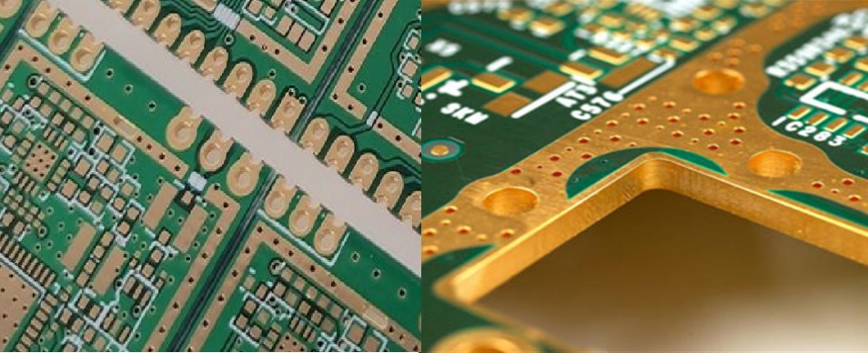
PCB edge plating and castellated holes are often seen in high-frequency circuit boards. High-speed digital signals generated by electromagnetic interference will not only cause serious interferences within the system, reducing the system's ability to resist interference, but also to the outside space to generate strong electromagnetic radiation, electromagnetic radiation caused by the system emits more than the EMC standard, so that the product can not be certified by the EMC standard. Multi-layer PCB board edge radiation is a relatively common source of electromagnetic radiation.
(1) Castellated holes
A castellated hole is a hole (drilling, gong slot) by the hole, followed by two drilling and shape processes, and ultimately, the castellated hole is retained. Metalized half-hole after sinking copper plate electricity, milling off the unwanted part, in the production process will produce burrs, off-set, etc. PCB half-hole molding, after plating makes the hole edge set with a tin layer, through the tin layer as a protective layer, enhances the tear resistance, can eliminate the hole wall of the copper layer, reducing the printed circuit board in the production process of impurities generated.
Castellated holes design is mainly used in Bluetooth, NBI0T modules, and other communication modules, core boards, can save connectors and space, generally appear in the signal circuit, which is characterized by a small aperture, hole metallization conduction, very much in line with the modern electronic circuits are only gradually sophisticated market demand. This type of PCB with a full row of semi-metalized holes on the edge of the board is characterized by a relatively small aperture, mostly used in carrier boards, as a motherboard sub-panel, through these semi-metalized holes with the motherboard and the components of the pins welded together.
Drill holes, chemical copper, full-board copper, image transfer, graphic plating, desmear, etching, resist soldering, surface treatment, molding.

(2) Edge plating
PCB gold-immersed edging refers to the side of the PCB that is also wrapped in copper skin, and the surface of the copper skin for the gold-immersed process, the top and bottom surfaces together. Design PCB edge plating process, the entire board edge with metal surrounded, so that microwave signals can not be radiated from the PCB board edge.
Edge plating as a circuit board special process in the mainstream production process is increasingly used in the present to minimize the size of the product at the moment, is used in equipment control motherboards and other products, due to electromagnetic interference and power integrity caused by the EMC problem is very prominent, multi-layer PCB board edge radiation is a relatively common source of electromagnetic radiation, metal cladding can be a good control of radiation.
In general,pcb edge plating usually have metal edges that provide additional protection and strong EMC for the board. The edge plating is usually made of copper or aluminum and have the following characteristics.
- Signal Integrity: Edge plating help maintain signal integrity through shielding.
- Physical Protection: Edge plating provides additional mechanical strength to the board, helping to minimize damage caused by external shocks.
- Enhanced EMC: Edge plating effectively reduces electromagnetic interference (EMI) and improves the board's electromagnetic compatibility.
PCB castellated holes and PCB edge plating production processes are similar, according to the current production process, there are restrictions on the spacing between the holes, and holes can not be made very small, at this time it is necessary to design the metal cladding to achieve the original requirements, gold-plated finger process can be realized by soldering the edge of the board wrapped in gold, but need to make a separate lead through the lead. For high-frequency and high-speed PCB board, the requirements of the board edge groove metallization, the formation of metalized edge grooves, the entire board edge package, microwave signals can not be radiated from the edge of the PCB board, but the need to consider the minimum distance from the nearby pads. The metalized edge wrapping process will increase the total cost of the PCB, which needs to be added to the project budget.
PCB can produce edge plating PCBs, we are committed to providing our customers with the most professional, high quality, customer satisfaction service, solving the customers' most concerned problems owning responsibility, standing with the customer, production, and restoring the customer's ideal design.