Via hole is a crucial element in PCB design, particularly in high-speed multi-layer PCB design, where the design of vias must be carefully considered by engineers. Let's delve into the knowledge of vias in PCB design.
Types of Vias
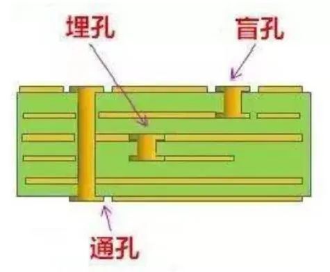
Vias are generally categorized into three types: Through-hole, Blind Hole,and Buried Hole.
1.Blind Hole: Refers to a hole that connects the top and bottom layers of a PCB but does not extend through the entire board. The depth of the hole is typically limited in ratio to its diameter.
2.Buried Hole: Refers to a via that only connects internal layers of a PCB and does not reach the surface.
3. Through-hole: This type of via goes all the way through the PCB and is used to achieve interconnection within the PCB or as mounting holes for components. Through-holes are easier to manufacture and are generally more cost-effective, so they are commonly used in most PCBs.

When designing and manufacturing PCBs, engineers must consider the following:
1. Vias should not be placed on pads.
2. There should be no vias within a 1.5mm radius from the component's metal casing where it contacts the PCB.
3. No vias should be placed within the area used for surface-mount adhesive or printing (e.g., under chip or SOP components).
4. The inner diameter of a through-hole should ideally be 0.2mm (8mil) or larger, and the outer diameter should be 0.4mm (16mil) or larger; in difficult cases, the outer diameter should be controlled to 0.35mm (14mil).
5. For BGAs with designs of 0.65mm or larger pitch, it is recommended not to use buried or blind vias as this significantly increases the cost.
6. The spacing between vias should not be too small to avoid hole breakage during drilling. Typically, the via spacing should be at least 0.5mm, and 0.35mm to 0.4mm spacing should be avoided. Vias with spacing of 0.3mm or less are not recommended.

Vias in Standard PCBs
In standard PCB design, the parasitic capacitance and inductance of vias have a minimal effect. For a 1-4 layer PCB, vias with diameters of 0.36mm/0.61mm/1.02mm (drill pad/POWER isolation) are suitable. For some special signal lines (e.g., power, ground, clock), vias with sizes of 0.41mm/0.81mm/1.32mm are better. Other sizes can be selected based on actual needs.
Vias in High-Speed PCBs
In high-speed multi-layer PCBs, vias are necessary for interconnecting signal traces between layers.Below 1GHz,vias are generally effective for connection,and their parasitic capacitance and inductance can be ignored.However,above 1GHz, the parasitic effects of vias can cause signal integrity issues,such as reflection,delay,and attenuation,due to impedance discontinuity.
When a signal passes through a via to another layer,the reference layer also serves as the return path for the signal,which can lead to problems like ground bounce.
Thus, in high-speed PCB design,seemingly simple vias can have significant negative effects on circuit performance.Engineers can mitigate these effects by:
1.Choosing appropriate via sizes.For typical multi-layer PCBs,vias of 0.25mm/0.51mm/0.91mm (drill/pad/POWER isolation) are preferred,while for high-density designs,vias of 0.20mm/0.46mm/0.86mm are used,or even non-through vias can be considered. For power or ground vias,larger sizes can help reduce impedance.
2.Increasing the POWER isolation zone and considering the via density on the PCB, usually D1 = D2 + 0.41.
3.Minimizing signal layer transitions to reduce the number of vias.
4.Using thinner PCBs to reduce the parasitic parameters of vias.
5.Placing power and ground vias as close as possible to their respective pins to minimize inductance.The traces for power and ground should also be as wide as possible to reduce impedance.
6.Placing ground vias near signal vias to provide a short return path for the signal.
In high-speed via hole in PCB design,via selection,minimizing the number of vias,and optimizing via placement are critical to reducing the impact of parasitic capacitance and inductance,ensuring signal integrity.