In order to take into account the development requirements of miniaturization, digitization, high frequency and multi-function, the metal lines on the PCB, as interconnection devices in electronic equipment, not only determine the opening of current,but also play a role. Signal transmission line. In other words, the power test implemented on the PCB circuit board responsible for transmitting high-frequency signals and high-speed digital signals must confirm the opening, closing and shortcut of the circuit on the one hand. On the other hand, it should also be ensured that the characteristic impedance never exceeds the adjustment range. In short, a board will never achieve required consistency unless two requirements are met.
The circuit performance provided by PCB circuit board must ensure that no reflection occurs during signal transmission. Signals remain integrated. Reduce transmission losses by achieving impedance matching. As a result, the transmission signal can be achieved holistically, reliably and accurately without interference or noise. Now we introduce the characteristic impedance control of multilayer boards with microstrip structures.

Figure 1 - Surface Microstructure
Surface Microstrips and Characteristic Impedance
Surface microstrips have high characteristic impedance and have been widely used in PCB manufacturing.The signal plane is set up as an outer layer of controlled impedance and insulating material used to separate the signal plane from its adjacent reference plane, which can be clearly seen in the image below.
Characteristic impedance can be calculated by the formula:
where Z 0 refers to the characteristic impedance. ε - [R to the dielectric constant of the insulating material.h is the thickness of the insulating material between the line and the reference plane. w to the width of the line. t refers to the thickness of the line. The image below clearly illustrates the meaning of each parameter.

Figure 2 - Parameters and meanings of formulae
Based on the formula shown above, it can be concluded that the elements that affect the characteristic impedance include:
A. Insulating material (dielectric constant ε - [R).
B. Thickness of insulating material (h).
C. Line width (w).
D. Line thickness (t).
It can be further concluded that the characteristic impedance is closely related to the substrate data (CCL data). Therefore, many factors must be considered in substrate material selection.
Dielectric constant and its effects
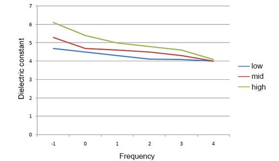
When the frequency is lower than 1MHz, material manufacturers measure the dielectric constant of the material. Due to differences in resin content, even the same type of material may differ from each other when produced by different manufacturers. Take epoxy glass cloth as an example. The relationship between the dielectric constant of epoxy glass cloth and frequency can be summarized as the following figure.
Obviously, the dielectric constant decreases with increasing frequency. Therefore, the dielectric constant of the insulating material should be determined according to the working frequency of the material, and the average value can meet the general requirements. As the dielectric constant increases, the signal transmission rate will decrease. Therefore, if a high signal transmission rate is required, the dielectric constant must be reduced. In addition, high characteristic impedance must be ensured for high transfer rates, which then depend on materials with low dielectric constants.

Figure 3 - Dielectric Constant versus Frequency
Line width and thickness
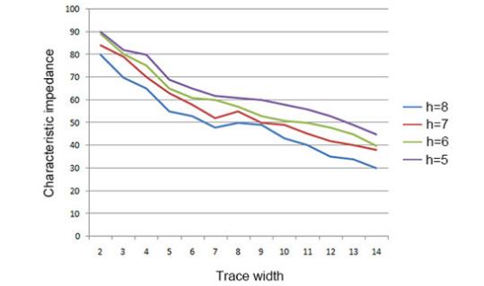
Line width is one of the most influential elements affecting characteristic impedance, and Figure 4 below shows the relationship between characteristic impedance and line width.
Based on Figure 4, it can be concluded that when the line width changes by 0.025mm, the impedance will subsequently change by 5 to 6 ohms. However, in actual PCB manufacturing, if a copper foil with a width tolerance of 18 μm is selected as the signal plane to control impedance, the allowed trace width tolerance is ±0.015mm. If you choose copper foil with a width tolerance of 35 μm, the allowed trace width tolerance is ±0.003mm. In summary, changes in line width will result in significant changes in impedance. The trace width is designed by the designer based on a variety of design requirements, not only to meet current capacity and temperature rise requirements, but also to bring the impedance to the expected value. Therefore, you must ensure that the trace width is compatible with the design requirements and within the allowed tolerances.
The line thickness also needs to be determined based on the required current capacity and allowable temperature rise. In manufacturing, coating thickness typically averages 25 μm. The line thickness is equal to the sum of the copper foil thickness plus the coating thickness. It should be noted that the circuit surface must be cleaned before plating to eliminate contaminants. Otherwise, the line thickness may be affected by non-uniformities, affecting the characteristic impedance.

Figure 4 - Relationship between Line Width and Characteristic Impedance
Thickness of insulation material
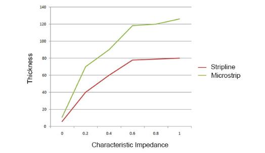
Based on the formula for calculating the characteristic impedance introduced above, it can be concluded that the characteristic impedance is proportional to the natural logarithm (h) of the thickness of the insulating material. Thereafter, larger "h" becomes larger "Z 0 ". Therefore, the thickness of the insulating material is also a key factor in determining the characteristic impedance. Since the line width and dielectric constant of the material are determined before manufacturing and the line thickness can be considered a solid value, controlling the characteristic impedance by controlling the stacking thickness is the main method. The relationship between line thickness and characteristic impedance can be summarized as the following figure.
It can be seen from this figure that when the thickness is increased by 0.025mm, the characteristic impedance will change by 5 to 8ohm. However, during the PCB manufacturing process, variations in the thickness of each laminate can cause huge variations. In fact, there are different types of prepregs selected as insulation materials in manufacturing, and the thickness can be determined by the number of prepregs. Take microstrip as an example. Figure 3 can be used to determine the dielectric constant of the insulating material based on the corresponding operating frequency, and then the characteristic impedance can be calculated. Then, based on the calculated values of line width and characteristic impedance, Figure 4 can be used to calculate the thickness of the insulating material,

Figure 5 - Relationship between Insulation Thickness and Characteristic Impedance
According to Figure 5 above, it is shown that the characteristic impedance of a microstrip structure is higher than a stripline structure with the same thickness of insulating material applied. Therefore, the microstrip structure is the first choice for high-frequency and high-speed digital signal transmission. Additionally, as the thickness of the insulation material improves, additional properties are added. Therefore, when it comes to high-frequency circuits with tight characteristic impedance, the CCL insulation material thickness must maintain tight tolerances, usually up to 10%. However, for multi-layer boards, the thickness of the insulation material is also a manufacturing parameter and should also be strictly controlled.
In summary, even small changes in line width, line thickness, dielectric constant and insulating material thickness can lead to changes in characteristic impedance. In addition to these factors, it is closely related to many more elements. Therefore, manufacturers must be fully aware of the components causing changes in characteristic impedance and adjust manufacturing parameters to keep the characteristic impedance within an acceptable range.
iPCB Circuits is currently able to manufacture PCBs with impedance control tolerances within the range of ±3%-±10%.