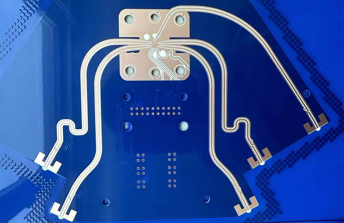
PCB in-board impedance refers to the true impedance of the traces inside the finished board, which is not the same concept as the traditional impedance strip (coupon). The PCB in-board impedance line and impedance strip impedance line there are alignment spacing, alignment width, alignment environment, alignment location and design errors, etc. will lead to the real impedance of the board and impedance strip impedance differences. However, with the current development of circuit boards towards high-density, high multi-layer, small volume direction, the customer impedance control requirements are becoming more and more stringent, the control accuracy requirements are also becoming more and more demanding. This PCB in-board impedance and impedance strip impedance deviation may be difficult for high-end customers to accept, more and more customers require PCB manufacturers to provide real PCB impedance through PCB in-board impedance test, rather than the traditional impedance strip.

PCB
What is the difference between PCB in-board impedance and impedance strip?
1, although the impedance strip and the real PCB board impedance line spacing, alignment width is the same, but the impedance strip test point spacing is fixed at 2.54mm (to meet the test probe spacing), while the real board end spacing is variable, with the emergence of QFP, PLCC, BGA packaging, some of the chip's pin spacing is much smaller than 2.54mm (i.e., the spacing of the impedance strip test point) spacing. The impedance strip alignment is a good choice.
2, impedance bar alignment is ideal for straight lines, while the real alignment of the board is often curved and varied. PCB designers and production staff can easily idealize the impedance strip alignment, but the real alignment on the PCB board will be due to a variety of factors leading to irregularities in the alignment.
3, the impedance strip and the real line on the board in the whole PCB board location is different. Impedance strips are located in the middle or edge of the PCB board, PCB boards are often removed by the manufacturer. The location of the real alignment is diverse, some near the edge of the board, some located in the center of the board and so on.
4, PCB board impedance alignment around the general distribution of holes, pads, mask layer, etc., while the impedance strip alignment around the environment are relatively single.
PCB in-board impedance test value of the impact of the board
1, impedance strip test point spacing impedance strip alignment spacing is different, will lead to test points and alignment between the impedance discontinuity. And the real differential PCB end (i.e., the chip's pins) spacing is often equal or very similar to the spacing of the alignment. This will lead to different impedance test results.
2. The impedance change reflected by the curved alignment and the ideal alignment is inconsistent. The characteristic impedance is often discontinuous where the alignment is curved, and the idealized alignment of the impedance strip cannot reflect the discontinuous impedance phenomenon brought about by the curved alignment.
3, the impedance strip and the real alignment on the PCB board in different locations. Nowadays, PCB boards are designed with multi-layer alignments and need to be pressed during production. When the PCB board in the compression process, the board in different locations by the pressure can not be the same, the thickness of the dielectric layer in different locations have differences, so the PCB board is often made in different locations on the dielectric constant is not the same, the characteristics of the impedance is also certainly different.
4, PCB board impedance by its surrounding holes, pads, mask layer, etc. reflects the impact of the impedance is not continuous, and impedance strip due to the alignment of a single environment, can not reflect the real changes in impedance.
It can be seen that the impedance value reflected by the impedance strip can not fully reflect the true characteristics of the PCB board impedance of the real alignment.
PCB in-board impedance test methods
The basic principle of TDR is that the step pulse generator sends out a fast rising edge step pulse. At the same time, the receiver module collects the time domain waveform of the reflected signal. If the impedance of the device under test is continuous, the signal is not reflected; if there is a change in impedance, the signal will be reflected back. According to the time of reflection, we can judge the distance of the impedance discontinuity point from the receiving end, and according to the amplitude of the reflected signal, we can judge the impedance change of the corresponding point.
With the current circuit board towards high-density, high multi-layer, small volume direction of development, the customer impedance control requirements are becoming more and more stringent, the control accuracy requirements are also getting higher, for example, precision requirements of less than ± 5%. PCB board impedance and impedance strip impedance deviation may exceed the control accuracy requirements, and the higher the control accuracy requirements, the higher the risk of using the impedance strip to assess the impedance.
Both PCB producers and high-speed circuit designers and manufacturers want to conduct TDR tests directly on real high-speed differential alignments within the PCB to obtain the most accurate characteristic impedance information.
There are two main reasons for the difficulty of PCB in-board impedance test:
1, it is difficult to find the ground point of the differential TDR probe. High-speed PCB designers will not place a fixed-pitch ground point near the end of the alignment (i.e., wafer pin) when designing a high-speed differential alignment.
2, the end of the differential alignment (i.e., the chip's pins or gold fingers or solder pads) spacing is variable, must be an adjustable spacing differential probe to realize the probe.