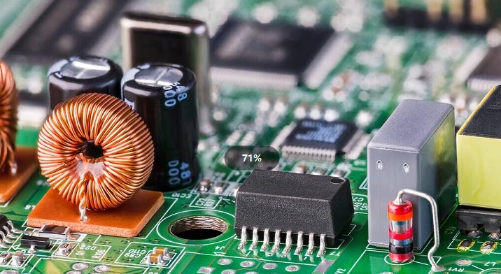
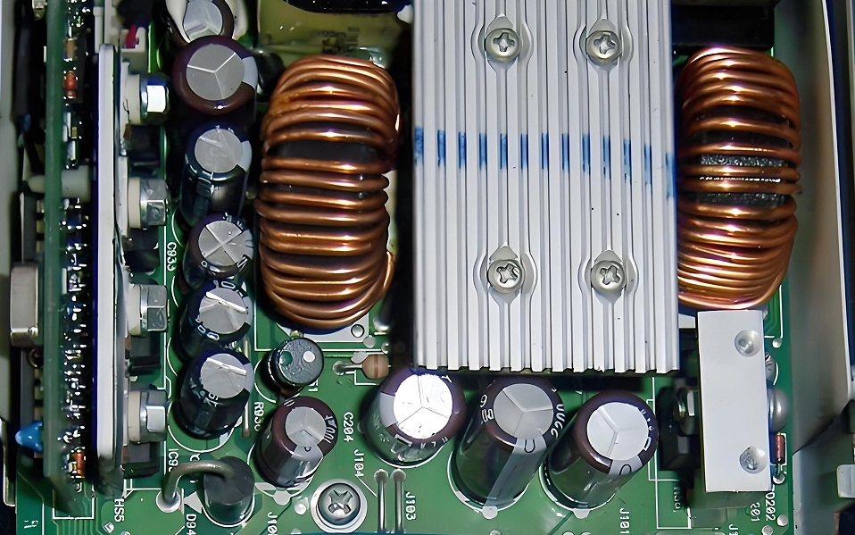
PCB inductor is the core energy regulation element in electronic circuits.
1. Basic principles and structure of PCB inductors
The work of inductors is based on the law of electromagnetic induction. When current passes through the winding, a magnetic field is generated around it, thereby converting electrical energy into magnetic energy for storage. According to structural differences, PCB inductors can be divided into winding type, laminated type, thin film type and other types. Winding inductors enhance the magnetic field through the magnetic core and are suitable for high current scenarios; laminated inductors use multiple layers of metal sheets for high-density mounting; thin film inductors use thin film technology to achieve miniaturization to meet high-frequency application requirements.
The performance parameters of inductors include inductance value (L), quality factor (Q), saturation current (Isat), etc. Among them, the inductance value determines the energy storage capacity, the Q value reflects the loss characteristics, and Isat characterizes the maximum current carrying capacity of the inductor before saturation. These parameters need to be accurately matched according to the circuit design requirements.

2. Classification and function of PCB inductors
-Power inductors
Power inductors are core components in power electronic equipment and are widely used in AC/DC converters, DC/DC converters and other scenarios. Its functions include:
Filtering: Separating high and low frequency signals by providing impedance to reduce power supply ripple.
Energy storage: Store energy when the switch is turned on and release it when it is turned off to achieve voltage conversion.
Transient response: Suppress current pulses and prevent instantaneous overcurrent.
Isolation: Reduce electromagnetic interference between input and output.
-Signal inductors
Signal inductors are mainly used for high-frequency signal processing, such as RF filters, LC oscillation circuits, etc. Its core parameter is the self-resonant frequency (SRF), and it is necessary to ensure that the operating frequency is lower than the SRF to maintain stable performance.
-Special inductors
Common mode inductors: Suppress common mode noise and improve signal purity.
Differential mode inductor: filter out differential mode interference and protect sensitive circuits.
Variable inductor: change the inductance value through mechanical adjustment to adapt to dynamic application requirements.
3. Layout and wiring principles of PCB inductors
Layout principles
Position optimization: the inductor should be as close to the IC as possible to shorten the current path and reduce parasitic inductance.
Magnetic field isolation: avoid arranging the GND layer or signal line directly under the inductor to prevent eddy current loss and signal interference.
Heat management: reserve enough space to ensure that the operating temperature of the inductor is within the rated range.
Wiring strategy
Line width design: select the appropriate line width according to the current size, for example, 2A current corresponds to 0.53mm line width (35μm copper foil).
Hot loop optimization: reduce the hot loop area and reduce EMI problems caused by parasitic inductance.
Signal shielding: high-frequency signal lines should be kept away from inductors, or a shielding layer should be used to reduce coupling effects.
4. Electromagnetic Interference (EMI) Suppression of PCB Inductors
The magnetic field generated by the inductor during operation may interfere with the surrounding circuits. The following measures need to be taken:
Copper skin treatment: remove part of the copper skin around the inductor to reduce the magnetic field radiation range.
Shielding design: use shielded inductors or add shielding covers to limit the magnetic flux lines inside.
Grounding optimization: ensure that the ground plane is continuous to avoid eddy currents caused by the magnetic field.
Auxiliary components: combine anti-shake capacitors, winding protection covers, etc. to further improve the anti-interference ability.

5. Application cases of PCB inductors
Power supply circuit
In switching power supplies, power inductors achieve voltage conversion by storing and releasing energy. For example, in a buck converter, the inductor works with the switch tube and the diode to ensure stable output voltage.
Communication circuit
In the RF front end, high-frequency inductors and capacitors form filters to suppress harmonic interference. For example, in mobile communication devices, inductors are used to select specific frequency bands to improve signal quality.
Automotive electronics
In vehicle power systems, inductors need to withstand harsh environments such as high temperature and vibration. For example, in DC/DC converters, high-temperature ferrite inductors are used to ensure long-term reliability.
6. Development trend of PCB inductors
As electronic devices develop towards miniaturization and high frequency, PCB inductors face the following challenges:
Miniaturization: Achieve smaller size through lamination and thin film processes to meet high-density integration requirements.
High frequency: Increase self-resonance frequency, reduce high-frequency losses, and adapt to applications such as 5G and millimeter waves.
Integration: Integrate inductors with components such as capacitors and resistors to reduce PCB area occupation.
Material innovation: Develop new magnetic materials to improve inductor performance and stability.
As a key component in electronic circuits, the design and layout of PCB inductors directly affect system performance. By reasonably selecting the type of inductor, optimizing layout and wiring, and strengthening EMI suppression, the stability and reliability of the circuit can be significantly improved. In the future, with technological advances, PCB inductor will play a core role in more fields and promote electronic devices to develop towards higher performance and smaller size.