As the most widely used interfaces in the world, Type-C and MIPI play a very important role in people's daily life, especially Type-C, which has made it mandatory for the European Union to let Apple iOS devices give up the proprietary Type-C interface, so if an engineer receives a design job about Type-C and MIPI interfaces, what should he or she do?

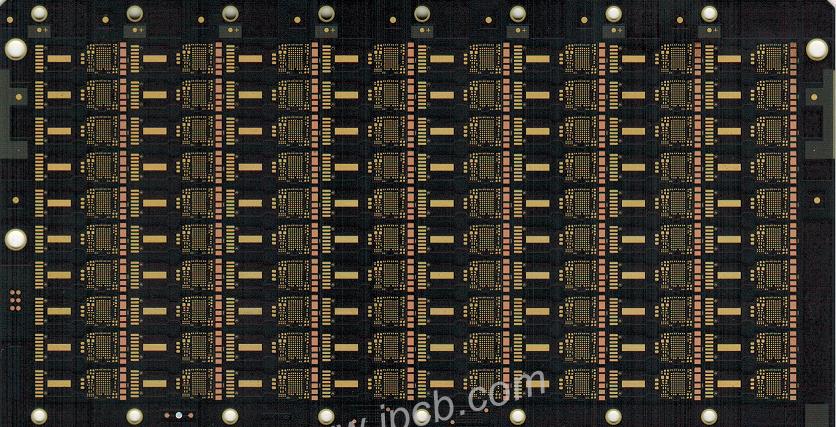
Type-C Circuit Board
Type-C
1.ESD, common-mode inductive devices close to the USB interface, placed in the order of ESD-common-mode inductive-resistive capacitive, the same should also pay attention to the distance between ESD and USB, leaving a distance of 1.5mm, but also consider the case of post-soldering.
2. Type-Ce has RX/TX1-2 four differential signals, two D+/D- differential signals, a total of six pairs of differential lines, the differential signal lines require at least immediately adjacent to a ground plane, two sides of the ground plane is best.
3. Ensure that the line spacing of the differential lines in the alignment process consistency, differential lines should be as far as possible equal length, if the two line length difference is large, you can draw a snake to add a new broken line length.
4. CC1/CC2 are two key pins, many roles: probe connections, distinguish between positive and negative, distinguish between DFP and UFP, that is, Vbus, the alignment of the surface to be coarsened.

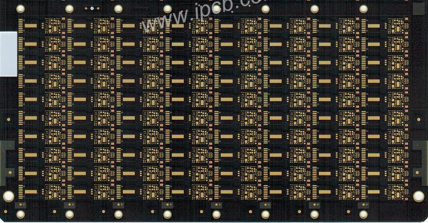
Type-C Circuit Board
MIPI Layout
1.Keep away from interference sources to prevent other signals from interfering with the transmission rate and quality of the signal.
2.All display interfaces (regardless of the interface or FPC form factor) should be placed as close as possible to the edge of the PCB board for ease of plugging and unplugging.
3. Don't put the main chip and display interface too far away from each other, and try to shorten the distance of the alignment, the alignment is a high-speed signal.
4.If the PCB has structural requirements, it should be placed in strict accordance with the structure.
MIPI wiring
1.MIPI impedance is 100ohm on PCB board.
2.Reference layer: In order to inhibit electromagnetic radiation, the MIPI differential line should be routed in the inner layer as much as possible, close to the GND plane, to ensure that the alignment does not cross the split, otherwise, it will cause discontinuity in the impedance of the differential line and the effect of new external noise on the differential line. If it is routed in the meter layer, it should be wrapped in the ground as much as possible to deal with it or to widen the distance with the other signals, and to ensure that it is more than 20mil.
3.Equal length: The length error between MIPI pairs should be controlled within 10mil, within 5mil, equal length is to ensure that the two differential signals reach the receiving end at the same time, otherwise it will not receive the correct data.
4.Symmetry: MIPI pairs should always maintain equal length and distance between pairs.
5.Principle of interference: MIPI line between the team to maintain more than 2 w distance, MIPI signal line theater in other high-speed signals (such as parallel data lines, clock lines, etc.), at least to ensure that more than 3 w distance must not go parallel lines, singling out switching power sources such as interference sources should be the principle.
6.Ground-packing: In order to prevent the antenna effect, there is no reference GND between the MIPI line every 50-100MIL to play a GND hole, to realize the three-dimensional ground-packing. The differential lines of MIPI signals should be minimized by punching holes for layer changing, as the holes will cause discontinuity in the impedance of the lines. If it is necessary to punch holes for layer changing for aligning the lines, ensure the consistency of the differential holes and arrange for a return ground hole near the hole changing position for signal return.