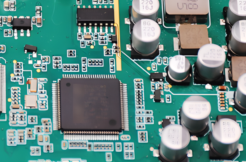
PCB board MI: Manufacturing instruction, refers to a variety of documents produced by engineering designers according to customer requirements and common industry standards and process requirements.
Via: A hole that only serves as a conduit,the connection of which must be two or more wires located in different layers.Through-hole generally change the soldermask ink, through-hole diameter is generally between 0.1-0.8mm,but pay attention to identify whether it is through-hole,need to be combined with the attribute marking and other information to help verify.
Component holes:used for component installation and welding,the hole ring needs to be designed as a soldermask window,holes' diameter is generally greater than or equal to 0.5mm.
Press-fit holes: welding-free holes,that is,the use of pressurized deformable pins cargo solid pins into the PCB plating holes to complete the contact connection, do not need to be welded by way of components and PCB connection.
Annular ring:the distance from the edge of the pad to the edge of the hole.
Pad: the end of the alignment,for component welding or line and hole connection.There are many shapes of solder pads, such as round, rectangular,square,etc.. Soldermask can be selected as either a soldermask opening or an ink cap.
Soldermask Clearance: soldermask opening,this means that the pads are not covered with soldermask ink,and the pads with open windows can be used for soldering components.
Soldermask dam:often refers to the soldermask ink retained between the IC foot and the SMD pad,the purpose is to prevent the solder bridge short circuit when soldering.
Trace spacing:the distance between neighboring wires.
Copper skin: refers to the copper surface with a relatively large area.
Outline line: refers to the profile line of the PCB, the contour line of the slot holes in the board.
Exposed line: refers to the soldermask opening due to oversize or alignment deviation caused by the pad adjacent to the wire or can not be covered by the soldermask.
Compensation: The purpose is to compensate for the reduced width of lines and pads caused by the etching process, which is pre-enlarged according to the copper thickness of the Gerber file provided by the customer, including lines, pads, etc., when the production file is made.
Haloing: refers to when the circuit substrate plate in the drilling, slotting and other mechanical action, once too violent, will cause the internal resin of the broken or small delamination of the phenomenon of cracking, called Haloing.
Pink Ring: multilayer boards within the laminate on the hole ring, and plating through-hole hole wall interconnections, the hole ring surface of the black oxide or brown oxide layer, due to drilling and plating holes in a variety of processes, so that the potion erosion and diffusion of the original color of the bare copper surface has become a circle, known as the “Pink Ring,” is a quality It is a kind of quality shortcoming, and its cause is very complicated.
Deburring: Refers to a variety of drilling, cutting, sawing and other processing, the edge of the material will produce hairy head or burr, the need to go through the details of the mechanical or chemical processing, in order to remove all kinds of small defects generated by the so-called “Deburring”. In circuit board manufacturing, it refers to the refurbishment of the hole wall or hole opening after drilling.
Dent: A gentle, uniform depression in the copper surface, possibly caused by localized pitting of the steel plates used for lamination.
Chamfer: In the gold finger area of the board edge, in order to make it easier to insert and connect the consecutive joints, not only to complete the work of cutting the beveled edge (Bevelling) in the front edge of the board edge, but also to remove the corners of the board or the direction of the slot (slot) mouth of the right angle, known as “chamfering”. It also refers to the chamfer between the end of the shank and the shank of the drill.

PCB board thickness greater than 1.0MM +/-10%, less than 1.0mm +/-0.1mm.
PCB warpage tolerance is less than or equal to 0.75%.
Line width/line spacing error +/-5% or less
PCB dimensions within +/-1.5mm
Hole and edge size tolerance of +/-0.1mm; hole position tolerance of +/-0.10mm;
When the hole diameter ≤ 0.8mm, the error between the part hole diameter and the designed hole diameter is between +/-0.05mm.
When the hole diameter > 0.8mm, the error between the part hole diameter and the designed hole diameter is between +/-0.1mm.