With the rise of the Internet of Things (IoT) and the increasing richness of mobile Internet content,people have put forward higher requirements for the transmission rate and service quality of mobile communication networks,and the fifth generation (5G) wireless mobile communication technology has emerged and been rapidly developed.At the same time,5G will also penetrate into various other industry sectors, and deeply integrate with industrial facilities,medical equipment,and vehicle networks to effectively meet the diverse business needs of the industrial,medical,and transportation industries, and realize the true “Internet of Everything”.
High-frequency millimeter wave has significant advantages in 5G communications, such as sufficient bandwidth,miniaturized antennas and equipment,and higher antenna gain. The U.S. Federal Communications Commission (FCC) plans four high-frequency bands for 5G,including three licensed bands (28GHz, 37GHz, and 39GHz bands) and one unlicensed band (64GHz-71GHz band),etc.However,it is a great challenge to find high-performance and affordable printed circuit boards (PCBs) in these bands.Therefore,it is important to understand the key parameters and characteristics of PCB materials and to select PCB materials that are suitable for use in the frequency bands used in 5G technology.
Loss
As circuits are designed to operate in the high frequency millimeter wave band,it is especially important to anticipate and control circuit losses.For high-frequency transmission lines and high-frequency circuit boards, insertion loss consists of dielectric loss, conductor loss,radiated loss, and leakage loss,and is the sum of the various loss components.Understanding these components is very helpful for circuit design.However,high-frequency PCB materials generally have large body resistance so RF leakage loss is very small and can be ignored.
Rogers has developed the MWI application software to simulate the various components of insertion loss,which can be downloaded from the Rogers homepage. It is based on the microstrip transmission line impedance and loss characterization method proposed by Hammerstad and Jenson,and tests have shown that the software simulations are highly accurate to the measured values.
Radiation Loss
As can be seen from Fig. 1,the total insertion loss of the microstrip line at 50 Ohm impedance varies with the frequency and thickness of the circuit operation. In order to avoid unwanted patterns (high radiation loss) in the microstrip line, a plate with a thickness less than a certain value should be selected according to the selected DK.In the case of 4350B,for example,a thickness of less than 1/80 of the free-space wavelength should be used to achieve negligible radiation loss. However, thinner dielectrics with narrower line widths and higher field strengths will result in greater conductor loss,and the roughness of the copper foil will have a greater effect on the conductor loss and the equivalent dielectric constant.The roughness of the copper foil also has a greater effect on the conductor loss and the equivalent dielectric constant.Therefore,a smoother copper foil is preferred for applications where lower losses are desired.This will be described later.When radiation loss is a design issue and the use of microstrip line circuits is not appropriate, GCPW transmission lines can be effective in minimizing radiation loss.On the other hand,any impedance mismatch in a transmission line is usually accompanied by some amount of energy radiation.Impedance mismatches are common in RF microwave circuit boards and are closely related to the specific design of the circuit and the Dk and thickness control of the pcb material.Selection of materials with tightly controlled Dk and thickness can minimize the mismatch due to variations in material tolerances, thereby reducing radiation losses.
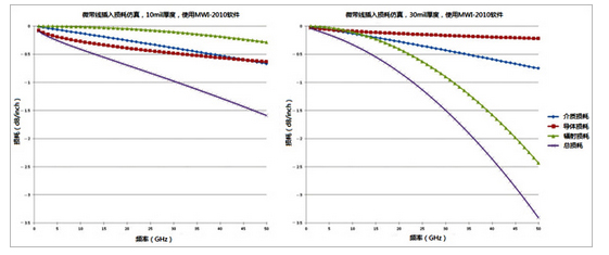
Fig. 1 Comparison of microstrip line insertion loss and components of DK 3.66, 1oz of the same material at different thicknesses
Copper foil roughness
Usually during PCB substrate processing,the surface of Cu foil is roughened to improve its bonding with the PCB dielectric material.However,a rougher copper foil surface will result in higher conductor loss, and the conductor loss will increase significantly as the frequency rises,which is caused by the skinning effect of the circuit. In general, the effect of surface roughness becomes significant when the circuit operating frequency corresponds to a trend depth less than or equal to the surface roughness of the copper foil.In the millimeter wave band, the trend depth is usually smaller than the surface roughness of the copper foil, e.g. 0.30um at 50GHz.
The surface roughness of copper foils can be measured in a variety of ways and units of measurement,and is usually expressed in terms of Root Mean Square Rq or RMS.By observing three types of copper foils (standard electrolytic copper, reverse processed copper,and calendered copper) under an electron microscope with the same magnification (7000x),the surfaces of the different copper foils exhibit completely different particle and roughness characteristics,as shown in Fig. 2. It is easy to find that the surface roughness of the standard electrolytic copper foil is higher, and the particles and contours are larger and deeper,while the surface roughness of the rolled copper foil is very small, and the particles and contours are very small,and the reversed process copper foil is in between the two.

Fig. 2 Comparison of surface roughness of different copper foils at 1/2oz thickness
By using Vececo's Wyko® NT1100 Optical Surface Profile Tester to measure the surface roughness value of copper foils, the root mean square value of the surface roughness of the above copper foils is 2.2um for standard electrolytic copper, 1.2um for a certain type of inverted copper, and 0.4um for calendered copper, by using different types of copper foils on the same material as that used for Rogers RO3003, the insertion loss is compared as shown in Fig. 3. A comparison of insertion loss for the same circuit using different types of copper foils on the same material as Rogers RO3003 is shown in Figure 3. The Rogers RO3003 material already has very low insertion loss characteristics using 1/2oz standard electrolytic copper, but the insertion loss is even lower using smooth 1/2oz rolled copper. This further illustrates that the smoother the surface of the copper foil selected, especially in the millimeter wave band,the more favorable the insertion loss reduction of the circuit.
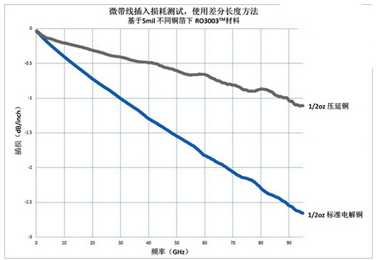
Figure 3: Insertion Loss Comparison of the Same Circuit Based on Different Copper Foil Types of 5mil RO3003 Material
Surface Finishing Process
The final surface finish of the circuit processing process also affects the circuit loss, especially in the high-frequency millimeter-wave band. Different surface finishes have different effects on PCB losses, which are more pronounced for broadband and high-frequency microwave circuits. The electrical conductivity of most PCB finishes is lower than that of copper foil. The lower the conductivity, the higher the conductor loss, and thus the higher the insertion loss of the circuit.
For high frequency circuits there are a number of different surface finishes to choose from, including electroless nickel-gold (ENIG), organic solder mask (OSP), electroless nickel-palladium-gold (ENIPIG), and soldermask. For example, ENIG (Electroless Nickel-In-Gold) is a chemical exchange method of plating nickel and then a thin layer of gold on the surface of a PCB copper conductor. Normally, the thickness of ENIG nickel is about 5um and gold is about 0.2um. Gold is a very good conductor, but the thin layer of gold is usually absorbed into the soldering point and disappears when the component is soldered to the PCB transmission line or lead wire.
Due to the skinning effect, at high frequency bands the current will travel along the surface of the conductor and the current will completely cover both the nickel and gold layers. Since nickel is less conductive than copper, circuits using the ENIG surface treatment will exhibit higher insertion losses than circuits using bare copper. RT/duriod® 6002 is a high reliability material used by Rogers for aerospace, satellite, etc., and the RO3003 product is a commercial grade material with essentially the same properties. The insertion loss characteristics of the same microstrip circuits made with different surface treatment techniques on 5 mil RT/duriod 6002 calendered copper were tested and compared as shown in Fig. 4. It can be seen that ENIG has the highest insertion loss, while the insertion loss of organic soldermask and chemically immersed silver is basically comparable to that of bare copper.
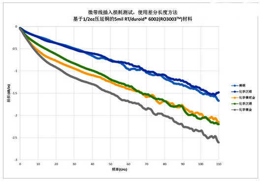
Fig. 4 Based on 1/2oz calendered copper 5 mil RT/duriod® 6002 (RO3003) material
Insertion Loss Comparison of Different Surface Finishes
Thermal Management
When high-frequency/microwave RF signals are fed into PCB circuit boards, a certain amount of heat will inevitably be generated due to the circuit itself and the wear and tear caused by the circuit materials. 5G equipment applications are not only increasing in frequency of use, but also miniaturization of the equipment, which will inevitably generate even more heat. Proper thermal management of circuits and understanding of the thermal characteristics of PCBs can help avoid deterioration of circuit performance and reliability due to high temperatures.
Thermal Modeling
A simple representation of the basic thermal model of a circuit and the heat flow profile model of a microstrip line is shown in Figure 5. In a microstrip circuit,the top signal plane is the heat source of the circuit and the bottom ground plane is the low-temperature region or heat dissipation plane, with the dielectric material filling between the two planes.In the thermal model,the heat will be transferred from the signal plane through the material to the low-temperature region of the ground plane to realize heat dissipation. Although the actual heat generation process in a microstrip circuit is complex,this assumption is acceptable for a simple thermal model. In the heat flow equation,k is the thermal conduction system of the material, A is the area of the heat source, L is the thickness of the material, and (TH-TL) is the temperature difference between the top and bottom. The heat flow equation and the thermal model explain that better heat dissipation and heat management can be achieved by choosing circuit materials with high thermal conductivity and thin thickness.
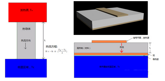
Fig. 5: Basic thermal model of the circuit
The (left) figure shows the basic thermal model,and the (right) figure shows the thermal profile model of the microstrip circuit
Thermal Management
Designers usually evaluate the temperature rise from the perspective of circuit efficiency and loss, but the PCB dielectric,as the nearest heat conductor to the heat source, is the part that has a greater impact on the temperature rise. As shown in Fig. 6, we can find through simulation that the method of reducing the temperature rise by lowering the Df value of a commonly used board is not as effective as the method of selecting a higher thermal conductivity (TC).Although the dielectric loss in different materials ultimately affects the insertion loss of the circuit,resulting in different heat generation,the thermal conductivity of the material is more significant to the temperature change than that of the material.For the same thermal conductivity value, e.g. 0.4 W/m/K, the temperature increase caused by a dielectric loss Df from 0.001 to 0.004 is only about 0.22°C/W.However,even for a material with a Df of the same 0.001,a change in thermal conductivity from 0.2 W/m/K to 1.5 W/m/K causes a temperature reduction of 0.82°C/W. If the input power of a circuit is 50 W,then the temperature can be reduced by 0.82°C/W.If the input power to the circuit is 50W,then the temperature can be reduced by about 40°C.
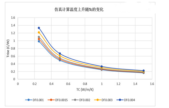
Fig. 6: Simulation of temperature rise with Tc and Df changes
In addition to the thermal conductivity of the material, some other parameters of the material also affect the thermal management. In order to better understand the influencing factors related to the thermal performance of PCB circuits, Table 7 shows the temperature variation results for circuits based on different materials, different material thicknesses, loss factors, thermal conductivity coefficients, copper foil roughness, and insertion loss. The table provides a reference for comparing the thermal effects of different circuit materials.The difference between the No. 1 and No. 2 circuits is the thickness of the circuits, so changes in the thickness of the PCB material will lead to differences in temperature rise. The thinner the thickness, the shorter the heat dissipation path,and the lower the temperature rise under the same conditions.Comparing Circuit No. 2 with Circuit No. 3, the difference is mainly in the insertion loss brought about by different copper foil roughness. The smaller the surface roughness of the copper foil, the lower the insertion loss and the lower the temperature rise;
Circuit 4 material is FR-4, which is basically not used in microwave/millimeter wave band.As an example it can be seen that FR-4 is deficient in a number of ways, such as high dielectric loss, conductor loss and low thermal conductivity, which results in the highest insertion loss for the same circuit, leading to a significant increase in temperature rise.Circuit 5 is based on Rogers RT/duroid6035HTC material, which has a high thermal conductivity of up to 1.44W/m/K for the best thermal conductivity characteristics, and at the same time has a very low loss factor,the lowest insertion loss, and the lowest temperature rise at the same input power, making it very suitable for high power microwave applications.

Fig. 7: Comparison of the heat test under different materials and thicknesses
Therefore,the heat management of circuits should choose relatively thin circuit materials, and at the same time, selecting materials with high thermal conductivity, smooth surface of copper foils, and low dissipation factor is beneficial to reduce the heat generation of circuits in the microwave millimeter wave frequency band.
Multi-layer board design
5G technology requires not only smaller base station equipment, but also smaller antennas. At the same time, active antenna systems (AAS), which combine active circuits and antennas, will be an important component of the upcoming 5G networks. The miniaturized design and the active antenna system will require circuits with more multi-layer board designs.
Z-axis coefficient of thermal expansion
The thermoplastic material typically used for high frequency PCBs is polytetrafluoroethylene (PTFE), which can be reinforced with various forms of fillers such as glass fibers or ceramic materials. PTFE thermoplastics generally have better electrical properties and lower electrical losses than thermosets, but the Z-axis coefficient of thermal expansion (CTE) of PTFE materials is considerably higher than that of copper. However, the Z-axis coefficient of thermal expansion (CTE) of PTFE is much higher than that of copper. In the production of multilayer boards, when the board passes through high temperatures, the different coefficients of thermal expansion of the material and copper will cause different expansion, resulting in the reliability of the PTH (Plated Through Hole) to be invalidated.
The importance of choosing a material with a low coefficient of thermal expansion for the reliability of plated through holes in high frequency multilayer board applications cannot be overstated.Rogers Corporation has found that the addition of special ceramic fillers to PTFE thermoplastic materials improves the coefficient of thermal expansion of the material. Combined with PTFE's inherent low temperature characteristics and electrical properties,this material is very suitable for high frequency millimeter wave multilayer board applications.For example,Rogers' RO3000® series circuit board materials have a Z-axis coefficient of thermal expansion as low as 24 ppm/°C.A simple plasma processing technique can be used to complete a highly reliable through-hole; and it has a very low dielectric loss (the dielectric loss of RO3003 is only 0.001 at 10 GHz),which is very suitable for high-frequency multilayer board circuit design.
Impedance Matching
The design and processing control of vias in HF microwave/millimeter wave multilayer circuit boards is also an area of concern.In the design and processing of vias, the size of the vias, the thickness of the copper inside the vias, the size of the pads on the outside of the vias,and the spacing between the vias and the ground plane all affect the parasitic capacitance and parasitic inductance of the vias.This affects the distribution parameters of the vias,resulting in an overall mismatch, which is more pronounced in the microwave/millimeter wave bands.A 7.3 mil Rogers RO4350B Lopro laminate was laminated on both sides with 8 mil RO4450F semi-cured wafers to form a 4-layer microstrip circuit containing through-holes.Through the experiment, we found that compared with the through-hole circuits, which have the same through-hole length and copper thickness,the circuits with smaller apertures and smaller hole pads have smaller parasitic capacitance,better broadband characteristics and return loss, as shown in Fig. 8, which gives the measured data of the impedance step change caused by reducing the through-hole apertures and hole pads to increase the return loss and RF bandwidth of the circuits.
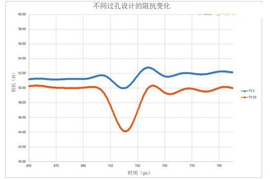
(a)
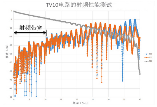
(b)
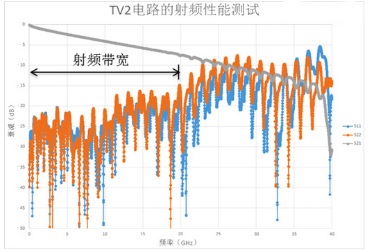
(c)
Fig. 8. Impact of through-hole impedance change on RF performance (a) Impact of different through-hole designs on impedance;
(b) RF performance test of TV10 circuit with large aperture;
(c) RF performance test of TV2 circuit with small aperture
In conclusion, the continuous development of 5G technology and the demand for microwave frequency bands have put forward higher requirements on the performance of PCB materials. Choosing the right board thickness according to the frequency, selecting PCB materials with low loss factor,understanding the effect of surface roughness of copper foil on PCB materials and selecting different copper foils, as well as suitable surface treatment techniques are favorable to reduce the insertion loss of the circuit. High thermal conductivity PCB materials are beneficial for heat management of smaller and more highly integrated circuits in 5G applications, enabling optimal heat dissipation solutions. At the same time, the right type of PCB material, the material's coefficient of thermal expansion,through-hole processing and reliability will ultimately determine the material selection.