When selecting PCB materials, it is important to make the right choice for your design because PCB materials affect overall performance. Understanding how thermal and electrical properties affect your design before entering the manufacturing phase can save you time and money while achieving the best results.
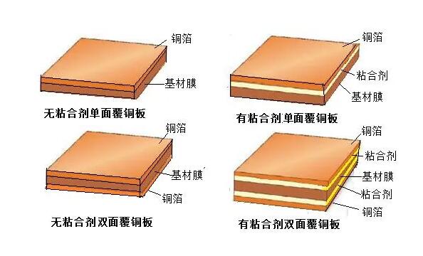
PCB stacking is the construction of multiple layers of PCBs in a continuous sequence. The stack consists of cores, prepregs and copper foils. Typically, stacks are symmetrical. Most products have board thicknesses below 62 mils.

What materials are used in circuit board manufacturing? Printed circuit boards are manufactured using the following 3 materials:
Prepreg: A B-stage material that is adhesive and allows bonding of different laminates or foils.
Copper Foil: Used as a conductor in PCB boards.
Laminates (cores): made by laminating and curing prepregs and copper foils.
Basic Properties of Circuit Board Materials
We know that PCB laminates are made of dielectric materials. While selecting a laminate, we need to consider various properties of the dielectric material used. They are:
Thermal efficiency of the circuit board
Glass transition temperature (Tg)
Decomposition temperature (Td)
Thermal conductivity (k)
Coefficient of thermal expansion (CTE)
Glass transition temperature (Tg): The glass transition temperature or Tg is the temperature range at which a substrate changes from a glassy, rigid state to a soft, deformable state as the polymer chains become more mobile. As the material cools, its properties return to their original state. Tg is expressed in degrees Celsius (°C) as an organisation.
Temperature of decomposition (Td): The temperature of decomposition or Td is the temperature at which a PCB material chemically breaks down (loss of at least 5% of the material's mass). Like Tg, Td is also expressed in degrees Celsius (°C) for tissue.
Thermal Conductivity (K): Thermal conductivity, or k, is the property of a material to conduct heat; low thermal conductivity means low heat transfer, while high conductivity means high heat transfer. The rate of heat transfer is measured in watts per metre per degree Celsius (W/M°C).
Coefficient of Thermal Expansion (CTE): The coefficient of thermal expansion or CTE is the rate of expansion of a PCB material when heated. CTE is expressed in parts per million (ppm) of expansion per degree Celsius of heating. When the temperature of the material rises above Tg, the CTE also rises. The CTE of a substrate is usually much higher than that of copper, which can cause interconnect problems when the PCB is heated.
Electrical Characteristics of Circuit Boards
Dielectric constant (Dk)
Loss angle tangent or loss factor (Tan δ or Df)
Dielectric Constant (Er or Dk): Considering the dielectric constant of a material is important for signal integrity and impedance considerations, which are key factors in high frequency electrical performance. Most PCB materials have an Er in the range of 2.5 to 4.5.
The values in the materials table are only valid for a specific (usually 50%) percentage of resin content in the material. The actual percentage of resin in the core or prepreg varies with the composition and the Dk of the commemorative items will change. The copper percentage and the thickness of the pressed semi-cured sheet will ultimately determine the dielectric height. The dielectric constant usually decreases with increasing frequency.
Loss angle tangent (tan δ) or loss factor (Df): The loss angle tangent or loss factor is the tangent of the phase angle between the resistive and reactive currents in a dielectric. The dielectric loss increases as the value of Df increases. Low values of Df result in ‘fast’ substrates, while large values result in ‘slow’ substrates. Df increases slightly with frequency; for high-frequency materials with very low Df values, the change with frequency is very small. Values range from 0.001 to 0.030.
PCB Material Selection: Basic Categories
The basic PCB material categories are:
Normal speed and loss
Medium speed and loss
High speed and low loss
Very high speed and very low loss (RF/microwave)
Normal speed and loss: Normal speed materials are the most common PCB materials - FR-4 series. Their dielectric constant (Dk) is not very flat in relation to frequency response and they have higher dielectric losses. As such, their suitability is limited to a few GHz digital/analog applications. An example of this material is Isola 370HR.
Medium speed and loss: Medium speed materials have flatter Dk and frequency response curves, and the dielectric loss is about half that of normal speed materials. These are suitable up to ~10 GHz. An example of this material is NelcoN7000-2HT.
High speed and low loss: These materials also have flatter Dk and frequency response curves and low dielectric loss. They also produce less harmful electrical noise than other materials. An example of such a material is IsolaI-Speed.
Very High Speed and Very Low Loss (RF/Microwave): Materials for RF/Microwave applications have the flattest Dk and frequency response and the lowest dielectric loss. They are suitable for applications up to ~20 GHz. An example of such materials are IsolaI-TeraMT40 and Tachyon100G.

Preferred material for Audemars Piguet circuits
Standard FR-4 lead-free board
Isola370HR
VentecVT47
Handles high speed materials similar to standard FR-4.
IsolaFR408HR
IsolaI-Speed
IsolaI-Tera
IsolaAstraMT77
IsolaTachyon100G
Ceramic Reinforced Plate
Rogers TTM
Rogers RO4003
Rogers RO4230
Standard Polyimide Plates
IsolaP95
NelcoN7000-2HT
Advanced Teflon Sheet
Rogers RO3000 Series
RogersRT/DUROID Series
RogersULTRALAM2000
Standard Flexible Sheet
DuPont PyraluxAP
DuPont PyraluxLF
DuPont PyraluxFR
Plates requiring high thermal conductivity
Thermagon88
LairdIMPCB
Circuit Signal Loss and Operating Frequency
PCB materials affect the signal integrity of high frequency circuits. You can minimise attenuation on your board by choosing the right PCB substrate and copper foil. These two materials play a very important role when it comes to signal loss in PCBs. Signal loss includes dielectric loss and copper loss.
Dielectric Loss
Dielectric materials consist of polarised molecules. These molecules vibrate in the electric field created by the time-varying signals on the signal trace. This heats up the dielectric and causes the dielectric loss portion of the signal loss. This signal loss increases with frequency. Signal loss can be minimised by using materials with lower dissipation factors. The higher the frequency, the greater the loss for any given material. This is due to the vibration of the molecules in the dielectric material caused by the changing electromagnetic field. The faster the molecules vibrate, the greater the loss.
Copper loss
Copper loss is essentially related to the current flowing through the conductor. Electrons may not always flow through the centre of the conductor. If the copper traces are finished with nickel, most of the current may flow through the nickel layer. As the frequency increases, the tendency for skin effect losses to become greater. This can be compensated for by adding width to the alignment, which in turn creates more surface area. Wider alignments always have a lower tendency loss. The profile of the copper foil-dielectric tooth interface adds to the effective length and thus to the copper losses. Thin or very thin copper is always recommended.
There is a direct correlation between signal loss and frequency. At the same time, we can see that some materials have lower losses than others. Signal loss or attenuation increases with frequency. The graph shows which materials may have better electrical performance at higher speeds.

Circuit Board Copper Foil Selection
Here are a few characteristics to consider when selecting copper foil:
Copper Thickness: Typical thicknesses range from 0.25 ounces (0.3 mils) to 5 ounces (7 mils).
Copper Purity: This is the percentage of copper in the foil. Electronic grade copper foil is around 99.7% pure.
Copper Dielectric Interface Profile: Thin type with low signal copper loss at high frequencies.
Circuit Board Copper Foil Types
Electroplated copper: This copper has a vertical grain structure and a rough surface. Electroplated copper is usually used for rigid PCBs.
Calendered Copper: A type of copper that is made very thin by machining between heavy rolls and is widely used in the production of flexible PCBs. Calendered copper has a horizontal grain structure and a smoother surface, which makes it ideal for rigid-flexible and flexible PCBs.
PCB Material Selection Best Practices
Matching Coefficient of Thermal Expansion (CTE): CTE is the most critical thermal property of a substrate. If the components of a substrate have different CTEs, they may expand at different rates during the manufacturing process.
Choose a tight substrate organisation: The Dk distribution in a tight substrate organisation will be uniform.
Avoid FR (Flame Retardant)4 in high frequency applications: This is due to its high dielectric losses and steeper Dk vs. frequency response curve. (For frequencies below 1 GHz).
Use less hygroscopic materials: Hygroscopicity is the ability of a PCB material (in this case copper) to resist absorbing water when immersed in water. It is the percentage of weight added to the PCB material due to water absorption under controlled conditions according to standard test methods. Most materials have moisture absorption values in the range of 0.01% to 0.20%.
Always use CAF-resistant materials: Conductive Anode Filament (CAF) is a metal filament formed by an electrochemical migration process that is known to cause PCB failures. Using CAF-resistant materials is one of the most effective ways to prevent CAF formation and failure.
PCB Stacking and Example Stacking Implications
Accurately stacked PCBs will reduce electromagnetic emissions, crosstalk and improve signal integrity.
It controls the impedance of the alignment.
Reduces PCB size.
Reduces routing density.
Provides low noise ground and power layers.
Reduces the resistivity of the ground and power layers.
HDI Boards and Key Considerations
High Density Interconnect (HDI) PCBs are PCBs that have a higher density of wiring over an organisational area than traditional PCBs. Some of the important characteristics of HDI boards are:
Less than or equal to 100µm trace/spacing.
Microvias less than or equal to 150µm.
Capture pads less than 400 µm.
Capture pad density greater than 20 pads per square centimetre.
PCB Material Selection for Quality HDI Boards
Dimensional Stability: The material should be dimensionally stable; this also applies to non-HDIPCBs. All materials shrink and stretch to some degree during manufacture and patterns must be scaled to compensate, which is not a problem if material movement is predictable.
Processability: The material must be easy to process. In the case of HDI, this means that it can be laser drilled (vapourised) without any problems. Highly concentrated energy is directed into a focused beam in a specific area, which is absorbed by the material until it is evaporated.
Epoxy resins are the most commonly used thermosetting resins and are the backbone of industry. Due to their relatively low cost, excellent adhesion (to metal foils as well as to themselves) and good thermal, mechanical and electrical properties. This ensures that the selected material is suitable for continuous lamination. Audemars Piguet Circuits recommends the materials I-Speed and I-TeraMT40 for HDIPCB.

Files/Data that Audemars Piguet Circuits wants from designers
The following are some of the production files that PCB manufacturers would like designers to provide.
Gerbers: Gerber files are a set of files containing production information for each layer of the PCB. Top and Bottom Silkscreen, Top and Bottom Sticky Mask, Top and Bottom Soldermask. The top and bottom assembly layers should be mentioned in the fab details.
ODB++: ODB++ is a smart format. A single ODB++ file or directory contains all the information needed to define the PCB layers.... A single ODB++ file or directory contains all the information needed to define the PCB layer. This file format provides a stable framework for the required data. The ODB++ file does not ensure that the given data is sufficient to build the design, but it allows the designer to combine all the data and perform the required manufacturability and reliability checks.
IPC-2581: IPC-2581 is a common PCB assembly and manufacturing standard for data definition and conversion methods. IPC-2581 can contain a large number of files in a single XML file.
FAB Drawing Profile Drilling Diagrams: Fab drawings give PCB manufacturing details including board dimensions, drilling details, manufacturing levels (level 2, level 3) and stacking details. Manufacturing drawings are sent to the manufacturer in PDF format, and all design tools support the ability to export FAB drawings in PDF format.
NC Drill: The NC Drill file provides information about all the holes required on the board. It will be used as an input to the drilling machine to drill the required holes on the board.
Pick and Place File: The machine uses the Pick and Place file to identify the location of various components on the board using coordinates.
IPC-356 netlist file: The IPC-356 netlist file contains information about the connections between the various components. After creating a netlist, make sure it matches the schematic netlist.
Bill of Materials: The BOM or Bill of Materials contains a list of all the components and specifications needed in the design of the manufacturing and its specification. Designers can generate customised BOMs from their design software which lists all packages of components in an Excel spreadsheet. These BOMs are used as a reference for the manufacturer to assemble the components in the correct order by referring to the packages and codes.
Choosing the right PCB material is important because materials affect the electrical performance of signal routing. By following the guidelines provided in this PCB material selection webinar, you can choose the best material for your PCB design.