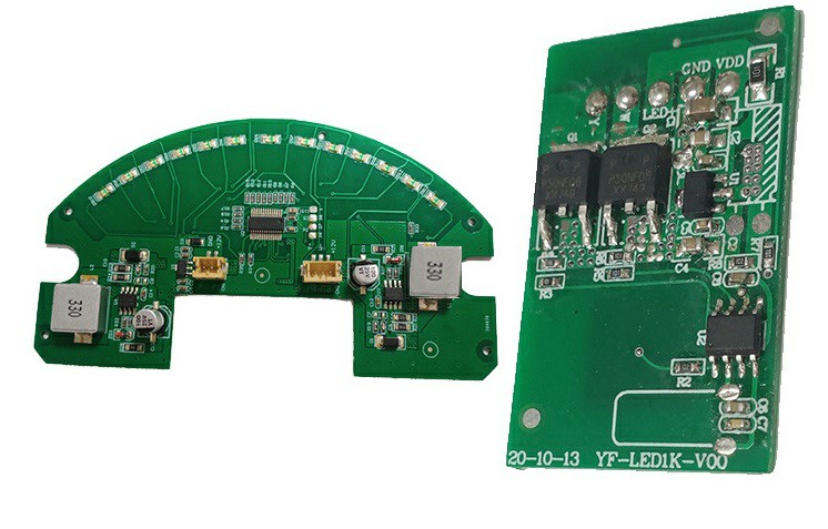
In the field of electronics manufacturing, printed circuit board assembly (PCBA) and reflow soldering process is inseparable from the two pillars of technology. PCBA as the “skeleton” and “nervous system” of electronic products, carrying the components of the electrical connection between the function; and reflow soldering is to ensure that these connections are stable and reliable core welding process. pcb reflow oven we will analyze the definition and process of PCBA, the principle of reflow soldering and technical points, as well as the synergistic relationship between the two, to reveal its importance in modern electronics manufacturing.
First, PCBA: the core of the assembly of electronic products
PCBA (Printed Circuit Board Assembly) refers to the electronic components through the surface mount technology (SMT) or through-hole insertion technology (THT) installed on the printed circuit board (PCB), and complete the welding process. Its core steps include:
(1) Solder Paste Printing: Accurately print solder paste on the PCB pads as a medium for subsequent soldering.
(2) Component placement: SMD components (such as resistors, capacitors, chips) placed on the pads through high-precision mounter.
(3) Soldering process: Divided into two major technologies: reflow soldering (for SMT components) and wave soldering (for plug-in components).
(4) detection and testing: the use of AOI (automatic optical inspection), X-ray inspection and other means to ensure the quality of welding.
The difficulty of PCBA is how to achieve zero-defect soldering in high-density, miniaturized design. For example, the motherboard of a modern smartphone may contain thousands of solder joints, and any false soldering or bridging will lead to functional failure.

pcba
Second, reflow soldering: precision soldering “temperature art" pcb reflow oven
Reflow soldering is the core soldering technology for surface mounted components (SMD) in the PCBA, which through precise control of the temperature profile, so that the solder paste melts and forms a reliable solder joint.The process can be divided into four stages:
(1) preheating stage: the temperature rises slowly to about 150 ° C,activate the flux and evaporate the solvent, to avoid thermal shock caused by component damage.
(2) Even heat stage: the temperature is stabilized at 170-200 ° C, to ensure that the PCB and components are evenly heated to reduce the temperature difference stress.
(3) reflow stage: peak temperature of 220-250 ° C, the solder completely melted and infiltrated pads, the formation of intermetallic compounds (IMC), which is the key to the strength of the solder joint.
(4) Cooling phase: rapid cooling down to solidify the solder to avoid grain coarsening leading to increased brittleness8.
Technical difficulties and solutions:
(1) Temperature profile optimization: parameters need to be dynamically adjusted according to solder paste composition (e.g., higher melting point of lead-free solder paste) and PCB heat resistance (e.g., high Tg boards).
(2) Prevent board bending and warping: 1.6mm thick PCB, reduce the size of the board, the use of overfurnace tray fixtures and other methods to balance the thermal stress impact.
(3) soldering defects control: such as cold soldering (temperature is not enough), bridging (solder paste excess) and other issues that need to be monitored in real time through SPC (Statistical Process Control).
Third, the synergistic effect of PCBA and reflow soldering
(1) the design phase of the mutual constraints
PCBA layout design directly affects the reflow soldering effect. For example, large-size PCB in the over-furnace easy to sag due to self-weight, need to be placed perpendicular to the long side and chain direction to reduce deformation. In addition, the thermal sensitivity of components (such as BGA chips) requires more accurate reflow temperature profile to avoid localized overheating damage to components.
(2) Material selection of the linkage
PCB board: high Tg value materials (such as Tg ≥ 170 ° C) can withstand higher reflow temperatures, reducing the risk of board warping.
Solder paste composition: lead-free solder paste (e.g., Sn-Ag-Cu alloy) is environmentally friendly but has a high melting point, requiring extended reflow time and possibly increased energy consumption.
(3) Typical cases of process synergy
Take automotive electronics PCBA as an example, it needs to meet the reliability requirements of high temperature and high vibration environment. Through the reflow process optimization (such as nitrogen protection to reduce oxidation), combined with the thick copper PCB design, can significantly improve the anti-fatigue performance of the solder joints.
Fourth, the future trend: intelligent and green manufacturing
(1) intelligent process control
Internet of Things (IoT)-based reflow oven can collect real-time temperature and humidity data, and through AI algorithms to predict welding defects and realize adaptive parameter adjustment.
(2) Environmental requirements drive innovation
The promotion of halogen-free solder paste and low-temperature soldering process is in line with the RoHS directive and also reduces energy consumption.
(3) Miniaturization challenges
With the popularization of 01005 package (0.4mm × 0.2mm) components, higher requirements for solder paste printing accuracy and reflow temperature uniformity.
The synergy between PCBA and reflow soldering reflects the deep coupling of the “design-material-process” trinity in electronics manufacturing. pcb reflow oven In the future, with the popularization of 5G, AIoT and other technologies, the two will continue to promote the evolution of electronic equipment to higher performance, smaller size, more environmentally friendly direction. Only through interdisciplinary technology integration and continuous innovation can we meet the increasingly complex manufacturing challenges!