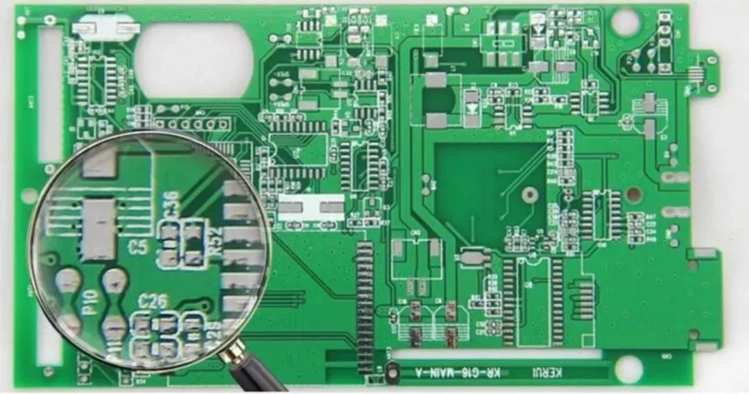
PCB silkscreen is the process of applying ink traces to a circuit board to identify its components, warning symbols,test points, markings, logos, etc. Typically, the component side is the one that is silkscreened by the manufacturer. It occasionally appears in the soldering channel, but achieving this is costly.PCB silkscreen helps manufacturers and designers quickly identify component layouts and ensures that parts can be reassembled. It provides engineers or technicians with instructions on where and how components should be placed on the PCB.
What is PCB Silkscreen?
Silkscreen on a PCB is a layer of ink printed on the surface of the board. It is usually made of a polymer or ceramic material and is applied using the silkscreen method. The ink is forced through a mesh screen, which acts as a stencil for the desired pattern. The screen is placed on the PCB, and the ink is applied onto the board. Standard colors used by manufacturers include black, yellow, and white. When using PCB software, a common font can be utilized in the design of the silkscreen layer. It is typically applied to the top and bottom layers of the board. Using silkscreen, text, labels, and symbols can be printed on the PCB surface, presenting information visually about component locations, part names, component numbers, brand logos, and more.

pcb silkscreen
Although the silkscreen layer does not affect the electrical operation of the board, it is critical to the processes of building, testing, and using the board. It helps to locate components and ensures everything is aligned neatly and in the correct orientation. This visual information is invaluable for the assembly process, providing easy-to-understand clues for technicians and assemblers. Now that you’ve learned the basics of PCB silkscreen, let’s explore its broader uses.
What information is available about PCB silkscreen?
PCB silkscreen may not influence the functionality of the board, but its value lies in the information it provides. For example, it helps anyone:
Warning Symbols: Identify warning symbols that highlight high-temperature components requiring user attention during operation.
Polarity: Understand component polarity to install components correctly. Pin markings provide orientation information for accurate assembly.
Test Points: Locate test point indicators on the silkscreen to assist design engineers with PCB testing and debugging.
Reference Indicator: Unique identifiers for each assembly location on the PCB that signify the component by a reference indicator.
Numbers: Unique numbers found on PCB silkscreen that indicate manufacturer markings, version numbers, etc.
Component Symbols: For specialized components such as diodes and optocouplers, symbols printed on the silkscreen ensure precise alignment during installation.
Switch Settings: Default switch settings are indicated on the PCB silkscreen, enhancing usability.
Dense Components: Pins on the silkscreen assist in testing and debugging compact component packages like ball grid arrays (BGAs).
Troubleshooting and Repair: Silkscreen markers make it easy to identify and locate individual components, speeding up the repair process.
Manufacturing Documentation: Silkscreen markers provide essential manufacturing and assembly documentation, including copyright notices, company logos, production dates, and other quality control details.
Branding: These markings contribute to PCB aesthetics and branding. Combining branding elements, logos, and selected colors enhances overall visual appeal and professionalism.