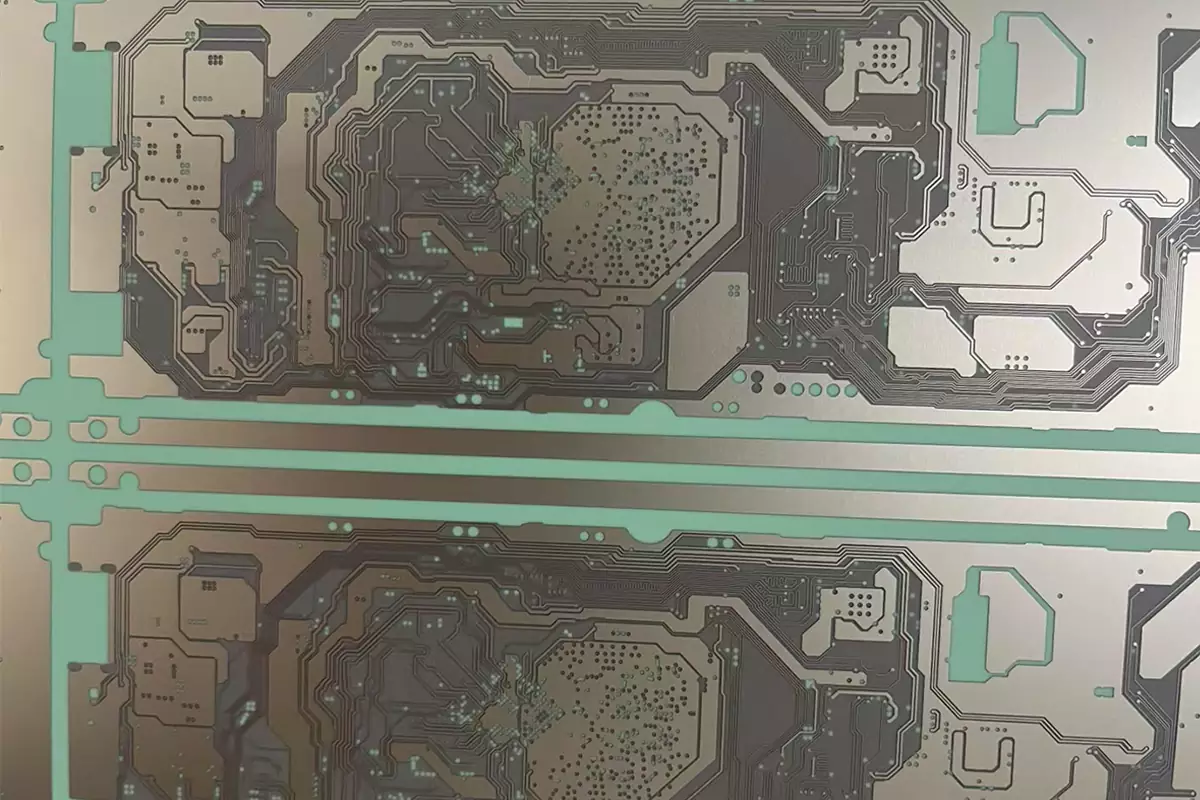
PCB lamination voids refer to the absence of epoxy resin in the circuit board. This can be detected when examining a cross-section of the circuit board under a microscope.
A detailed understanding of voids, their root causes, and prevention methods will help manufacture high-quality PCBs. There are different types of voids in circuit boards (plating voids, annular voids, wedge-shaped voids, etc.).
What are lamination voids in PCB manufacturing?
Voids occur during the board lamination process due to the absence of resin at the interface of the adhesive material. In some cases, lamination voids can also be caused by the underlying raw materials. The delamination process between the dielectric and copper foil can cause cracks in the inner metal foil.
What is PCB delamination?
When a corrosive medium is allowed to directly contact the metal substrate, then in the presence of water, an electrochemical reaction occurs at the metal-coating interface, causing delamination. Delamination refers to the loss of adhesion between the coating and the surface or between the coatings themselves.
Delamination between the dielectric and copper foil leads to foil cracks and barrel cracks. When stress is induced in the substrate, the via resists this change, but this resistance can result in barrel cracks in the circuit board. What causes voids in PCB lamination?
1. In some cases, the CTE (coefficient of thermal expansion) of different materials, such as glass and resin, does not match. When stress is applied to the substrate, its CTE rises above its specified glass transition temperature (Tg). Stress on the plated through-holes occurs due to strain in the Z axis.
2. The prepreg is not from the same material.
3. Incorrect orientation. The grain orientation of the prepreg and core material should be consistent. Resin substrates are anisotropic, meaning they have different values in different directions (determined in the warp and weft directions).
4. Lamination parameters such as vacuum, temperature, and pressure (calculated based on the material's Tg) are incorrectly calculated.
5. The laminate profile changes with environmental conditions and machine parameters. Therefore, the profile must be set before processing begins.
6. Incorrect drilling values.
7. Regarding circuit design, if the copper distribution is uneven, resin recession can occur. Therefore, you need to add sufficient copper mesh (in areas not needed in the circuit) to balance the copper.

PCB
Cross-section of a plated through-hole in a PCB:
1. To investigate the effects of voids, void shape, and void size, consider the distribution of voids within the critical volume.
2. Barrel cracks and foil cracks are causes of improper lamination. If cracks occur at the knee of the hole, microscopic cross-sectioning is necessary for detection.
3. At the interface of the adhesive effect, laminate voids affect thermal conductivity, bond strength, and stress decoupling.
4. Because voids impede heat flow from the board to the heat sink, they lead to temperature fluctuations and reduced bond strength.
How to reduce voids in PCB laminates?
1. Increase the average resin pressure by applying a higher consolidation force or restrict resin flow to reduce pressure gradients.
2. Increase resin outflow from the laminate to promote the elimination of mobile voids. Reducing the cure pressure creates an environment that is favorable for void formation. At low cure pressures, you can restrict resin flow and increase the average resin pressure in the laminate. This promotes resin outflow, allowing voids to be removed from the laminate along with the resin. 3. Restricting resin flow in laminates reduces the average characteristic void diameter from 200μm to 166μm, while increasing void content from 5.5% to 7.3%.
4. Void content increases with increasing air escape path length. Since voids are pockets of air trapped during the lamination process, the best way to minimize void formation at low lamination pressures is to stack/press the laminates in a vacuum.
5. Void content increases with increasing laminate dimensions. This is because the air escape path length is longer.
PCB Cracking and PCB Adhesion Deficiency
During the lamination process, resin flows out to fill voids between adjacent layers. When this flow occurs, if there isn't enough resin in the prepreg, the glass fibers will come into contact with the copper layers. This is known as adhesion deficiency.
Because the dielectric breakdown threshold of glass is lower than that of resin, the dielectric may crack. Additionally, if there isn't enough resin to fill the voids between adjacent copper layers, air-filled bubbles will form. Furthermore, when the drill penetrates these bubbles, chemicals become trapped within them and can cause degradation of the plated through-hole. If there isn't enough resin to withstand the stresses of the drilling process, microcracks in the glass fibers begin to develop, leading to cathodic anodic filamentation (CAF), also known as cracking.
Conductive Anodic Filament Formation
Most actual CAF growth is caused by accelerated humidity and temperature test conditions. It can be easily traced back to a lack of resin covering the glass.
Glass stop occurs when there isn't enough resin to cover the etched copper, roughness, and glass. It paves a pre-existing path for moisture intrusion in humid environments, leading to CAF growth and failure under applied voltage bias.
Eliminating voids at interfaces will improve the quality of laminate composite structures. Reducing void content leads to increased adhesive shear strength and reduced laminate thermal resistance. These critical metrics contribute to improved component reliability and greater electronic performance.
If you have any questions about PCB lamination voids, please contact iPCB for professional solutions and expertise.