5G wireless networks cover a wider frequency band,placing special demands on circuit board materials for 5G circuits operating at millimeter-wave frequencies.This paper discusses the effect of the external finish of the inner wall of the metallized vias used to transmit signals in the channel between the top and bottom copper foils of a PCB material on the final RF performance of the material.
Fifth-generation wireless networks have been hailed as one of the most critical technological achievements for the successful realization of modern communications. 5G technology utilizes both signal frequencies below 6 GHz and millimeter-wave frequencies for short-range backhaul, high-speed numerical links. Circuits in such a wide frequency range require the use of special circuit board materials,and Rogers Enterprises' RO4730G3 circuit board material has become the choice of many circuit design engineers due to its exceptionally good performance from RF to millimeter-wave frequencies.However,one difference between this laminate material and traditional circuit materials is that the material utilizes hollow microspheres as a supplemental material to the medium, a difference that has caused a bit of concern among circuit presetters.
Because of the presence of the microspheres,the appearance of the circuit processing structure-such as the metallized vias (PTHs) that run from one conductive layer to the next-appears to be much better than that of conventional circuit board materials that do not use this special media filler as they see fit.The metallized vias are less delicate than those created by conventional circuit board materials that do not use this special media filler as deemed appropriate. This may appear to be the case, or there may be some other concern, since the metallization of circuit boards using hollow microsphere fillers is considered to be very poorly textured. However, a series of studies have shown that the effect of hollow microsphere filler on the metallized holes is purely cosmetic and does not affect the performance of the circuit or the reliability of the metallized holes, no matter at RF frequencies or millimeter-wave frequencies for 5G wireless networks.
Comparison of Different Metallized Vias
The texture of the wall surface of all metalized holes in a circuit varies slightly,even when comparing the finish of holes in the same circuit board. Because the drilling process involves a number of factors, the appearance of the metallized hole wall varies from hole to hole. In materials with microsphere fillers,the drill bit may or may not affect the microsphere fillers, thus creating a difference. When the drill bit strikes and breaks a hollow spherical cube, the copper plating of the hole will grow along the approximate contour of the broken spherical cube, and the hole wall appearance will no longer be smooth and bump-free. Fig. 1 shows how the presence of microsphere fillers in a circuit board affects the increase in appearance finish caused by the formation of metallized vias in the circuit material. It is natural to question whether this finish will have a negative impact on the electrical performance or reliability of the circuit compared to the smoother appearance of conventional circuit materials with metalized perforations.
As the need for high-frequency circuit materials with a wide frequency range for 5G wireless networks is increasing day by day, it is meaningful to understand whether the finish of metallized perforations in circuit board materials with hollow microsphere fillers,which are not present in conventional circuit board materials, has an impact on circuit performance.After a series of investigations, a comparison was made to see if the difference in via wall finish of 20.7 mil thick RO4730G3 circuit board material with glass reinforcement and microsphere filler from Rogers Enterprises would have an effect on the circuit performance compared to 20 mil thick RO3003G2 material without glass reinforcement and with smaller, non-hollow filler. In order to test for the effect of hole wall finish, a number of different test circuits have been developed to compare the behavior of metallized vias on circuit boards over a 5G wide frequency range.
The test circuits are based on a microstrip channel transmission line structure with a through-hole in the mid-circuit half-waist that serves as a conductor and signal transition from the top copper layer of the dielectric substrate material to the copper layer at the end. The length of the test circuit is basically about 2 inches.We also used a little bit of other high-frequency channel transmission line technology as a reference to evaluate if there was an effect on the exterior finish of the metallized via walls, covering 8-inch and 2-inch lengths of microstrip circuits without signal vias, and 8-inch and 2-inch lengths of Ground Common Plane Waveguide (GCPW) circuits without via holes. In order to ensure complete homogeneity during testing, the test utilizes the same two 2.4 mm coaxial connectors for all circuits. The test connectors are always connected to the test ports of the VNA in the same manner to maintain phase uniformity.
Those accustomed to the task of examining the predefined micrographs of printed circuit boards (PCBs) shown in Fig. 1 are likely to be concerned about the impact of the finish of the metallized vias, especially at the high frequency of 5G circuits. Generally speaking,for conventional HF circuit materials that do not utilize microsphere supplements, the lack of a fine hole wall appearance may mean that certain issues have been revealed during the manufacturing process and may affect the reliability of the vias. However, the formation of metallic vias with a non-fine appearance is normal for hollow microsphere-supplemented circuit materials, and this does not mean that they have poor performance.
In order to confirm that the non-delicate metallized perforations in this circuit material do not affect the reliability and electrical properties of the perforations, we have compared the new material (less delicate metallized perforations) with more conventional circuit materials (smoother metallized perforations) to eliminate any concerns about the use of this material in the 5G wireless network circuitry pre-design and in other circuits wherever millimeter-wave frequency ranges may be applied. The following are some examples of the use of millimeter-wave frequency range circuits in 5G wireless networks
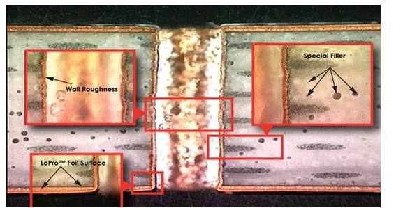
Fig. 1. Compared to the circuit material without microsphere filler, the RO4730G3 circuit material with hollow microsphere filler has the potential to form metallized perforations with non-fine pore wall appearance.
Prior to evaluating the effect of metalized vias and their wall appearance on the performance of high frequency circuits, an extensive evaluation of the RO4730G3 circuit board and its microsphere filler was performed to fully understand their specific properties under different office conditions.A series of material testing studies were conducted covering 10-layer Highly Accelerated Thermal Shock (HATS) / Metallized Through-Hole (PTH) reliability,double-sided PTH reliability, double-sided PTH-PTH conductive anode filament (CAF) resistance, simplest side-simplest side CAF resistance, MOT and surface-to-surface-mount (SMT) testing, insulating resistance,and metallized through-hole quality,among others.A series of material testing seminars. All the tests showed that the materials passed these tests without any problems under the industry standard test conditions for microsphere fillers.
Our focus is to introduce the question of whether it is possible to sprout problems by utilizing the material at RF, microwave and millimeter wave frequencies.
As a matter of fact,in a number of research tests conducted on this circuit board material with its microsphere filler in mind, the various effects of changes in the external finish of the metallized perforated wall on RF performance were compared using two materials with different metallized perforated wall feature marks. The research tests are based on a special pre-designed microstrip channel transmission line circuit with microstrip line circuits on the top and bottom layers, respectively,with the half-waist medium being the mediator material, and the connection of the microstrip line from the top layer to the end layer is successfully achieved through the metallized perforation. These tests are intended to provide a very meaningful numerical reference for 5G applications,as the test circuit has satisfactory RF performance in the 100 MHz to 40 GHz range.
The dielectric constants (Dk,or εr) of the two materials utilized in the study were very close to each other, with values in the vicinity of 3. Both materials were also chosen to be of the same thickness, 20 mils. Both materials were also selected to have the same thickness,20 mil, with the main difference being that one produced a smooth metalized perforation, while the other produced a less fine metalized perforation.The material that can produce a smooth metallized perforated wall appearance is RO3003G2 circuit board material from Rogers Enterprise, while the RO4730G3 circuit board with glass reinforcement and hollow microsphere filler produces a less delicate metallized perforated wall appearance.
Textural differences in the appearance of metalized perforated walls in circuits are generally thought to be a problem of the circuit fabrication rather than the material. However, there are a number of material-specific properties that can optimize the appearance of metallized perforated walls, including circuit material filler type, filler size, glass reinforcement, and natural resin type. As RO4730G3 circuit board and its hollow microsphere filler (non-delicate metallized perforated wall appearance), the comparable RO3003G2 circuit board material does not have glass reinforcement and the filler particles are very small. If both are considered suitable and the optimum PCB processing method is used, the latter will have a very flat and smooth metallized perforated wall appearance. As shown in Figure 2, the RO3003G2 PCB can be formed with a very smooth metallized via wall.
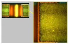
FIG. 2. Micrographic image revealing the smooth-appearing metallized perforated aperture walls formed in a 20 mil thick RO3003G2 circuit material.
For the same thickness of these two circuit materials, the difference in the appearance finish of the metallized vias for the two materials shown in Figures 1 and 2 is quite obvious. A closer look at the two figures may lead to the question of whether the higher finish of the metalized vias means that there is something wrong with their RF performance. For test circuits, microstrip conveyor line circuits are a useful way to compare the effect of a smooth and unglossy metalized via wall appearance on RF performance, since a small change in the processing of the microstrip line has less effect on RF performance than other high frequency conveyor line configurations.
In order to provide meaningful final results for metallized vias in different circuit materials at 40 GHz, we have invested a great deal of effort in optimizing these individual microstrip circuits. One of them is the signal transition from the RF test connector to the PCB microstrip line which is a big challenge by default. In general, it is not easy to get a good return on the signal transition of a microstrip conveyor line on a 20 mil thick board with special characteristics, especially for frequencies above 25 GHz. For broadband microstrip circuits, return losses of less than 15 dB or better are generally considered acceptable.
Through-hole transition is another critical consideration, especially at millimeter-wave frequencies where it is more difficult to successfully achieve low-casualty transitions from one layer to the front circuit layer. Generally speaking, it is difficult to successfully achieve satisfactory performance of microstrip through-hole transitions above 20 GHz on 20 mil thick circuit materials. However, considering the difficulties mentioned above, the microstrip first test circuit in this study is designed to achieve satisfactory results even at frequencies up to 40 GHz, as shown in Fig. 3.
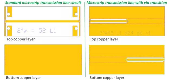
Fig. 3. These circuits were used to evaluate the circuit defaults for the effect of the external finish of the metalized aperture walls on RF performance at high frequencies, with a standard microstrip channel transmission line on the left and a microstrip line circuit with metalized apertures on the right.
The “standard” microstrip line circuit shown on the left in Figure 3 is a microstrip circuit that successfully realizes signal transition conversion by means of a grounded coplanar waveguide (GCPW) structure. The main body of the circuit consists of a microstrip channel transmission line, and the GCPW structure is used at the end of the circuit for coaxial (2.4 mm) connector-to-microstrip transition conversion (Southwest Microwave model #1492-04A-5). The circuits on the right side of Fig. 3 are the top and bottom circuits used in the test circuits of this study. They are loosely coupled grounded coplanar waveguides with metalized vias halfway down the midsection to provide transition connections from the top layer to the end layer circuits. With a test circuit length of 2 inches, the loosely coupled grounded coplanar waveguide conveyor line circuits will have very similar RF performance as the microstrip conveyor line circuits. The loose coupling has satisfactory performance at higher frequencies and is well suited for testing at 40 GHz.
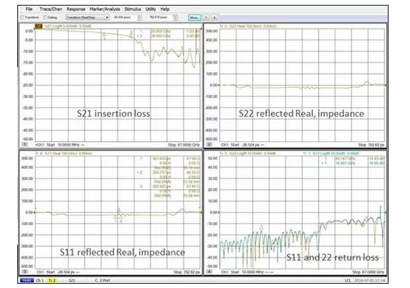
Fig. 4. This is an illustrative example of S-parameter variables obtained from network profiler tests for metallized vias with different circuits and different wall-exterior textures, covering the frequency and time domains, respectively.
Fig. 4 shows the final results of the vector network profiler in the frequency and time domains.The two marks in the lower right corner of the figure for the return casualties (S11 and S22) express the return casualty values at different frequencies respectively. Marker 2 is located at 40.7 GHz, which is the infinite frequency at which the test circuit has a satisfactory return dropout. The impedance of the reflected wave S22 is shown in the upper right corner of the figure, and the impedance of the reflected wave S11 is shown in the lower left corner of the figure. As shown by the marking of S11,the impedance values in the through-hole transition,markings 1, 2 and 3, the circuit has an impedance of about 48? Smaller impedance variations can be measured in the range of through-hole transition areas, with impedance variations of less than 2 bars, which have almost no effect on the RF performance of the circuit. From the final results of these tests, the circuit can be seen to have satisfactory through-hole transitions from the top to the end signals, and at the same time,it also has satisfactory insertion and depletion performance up to 40 GHz (shown in the upper left corner of the figure).
A number of circuits of the same preset were fabricated on the same large PCB in order to better understand the changes in RF performance caused by normal material variations as well as variations in the PCB fabrication process going forward. We processed two large PCB boards (Board 1 and Board 2) at the same time, on which powdered and water-fermented foodstuffs containing multiple test circuits were fabricated, and both large boards came from the same piece of circuit material with the same and larger plane or object surface size.
The original size of the material for the larger board was 24 x 18 inches, which was cut into two wrenches both measuring 12 x 18 inches, as the two 12 x 18 circuits from the same board were able to maintain the exact same material. In the fabrication of the two selected microstrip line test circuits in 20 mil RO3003G2 and 20.7 mil RO4730G3 materials, absolutely identical circuit machining fabrication processes and procedures were utilized as deemed appropriate to minimize the impact of machining.
Comparison of final test results
After examining the circuit materials tested, a large number of test values were obtained for each of the test circuits covering: insertion depletion, return depletion, impedance, group delay and phase angle (as shown in Figure 4). Straight-through surveys are used as a means of confirming the effect of metalized vias on circuit performance. The impedance of the circuit is also measured, but is not considered to be the best indicator of the effect of metalized vias on RF performance. The impedance of a microstrip line circuit (or a loosely coupled grounded coplanar waveguide) is affected by parameters such as medium thickness, conductor width, copper thickness variation, and medium Dk in that order. The impedance in the transition area of the metallized vias will be more affected by these individual variables than by the effect of the exterior of the metallized vias' walls. For the reasons stated above, the impedance is not used to determine the effect of the exterior of the metalized aperture wall on the RF performance, although the impedance value is achieved by aggregation.
The phase angle of S21 is used as the air degree of RF changes in the circuit induced by changes in the appearance of the metallized aperture wall, since the conductor appearance finish along the microstrip conveyor line will affect the phase angle of the signals through the conveyor line.1,2 The through-hole survey is more sensitive to the RF signal paths that have a change in the through-hole. To verify the correctness and repeatability of the test, a repeatability study where the test circuit was uplinked found that the standard deviation of the S21 phase angle at 39 GHz was less than ±1.2 degrees. The S21 phase angle we utilized in the test is the spreading phase angle of S21, which is the full value of the -180 to +180 degree phase angle. It is considered appropriate to use this approach to be more meaningful in terms of increasing the defense rate, since the defense rate is less sensitive to non-expanded phase changes, even for frequencies up to 39 GHz in 5G applications. However, for a 2-inch long microstrip channel transport line on a circuit board stock with a Dk of about 3, the spreading phase angle range at 39 GHz will be in the thousands of degrees, as this test circuit and survey solution can be used to give suitable phase defenses.
While the values aggregated in the metallized perforated hole wall study are very broad, it is still possible to share a few final results here. For example, FIG. 5 shows the values for six different circuits of the same preset fabricated on the same board, and compares them to a microstrip channel conveyor line without through-hole transitions as a reference. Fig. 5 also shows the values of six different circuits manufactured on a second board with the same pre-design (both boards were initially cut from the same 24×18 piece of material). The final results of the test were based on 20 mil RO3003G2, which has a flat and smooth metalized perforated hole wall appearance.
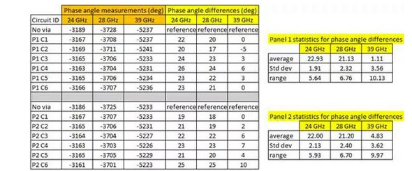
The phase angle survey developed by S21 shows a 2-inch long microstrip channel transmission line circuit including metalized perforations. The circuit board material is RO3003G2 with a thickness of 20 mils, which gives a very smooth appearance of the metalized perforated walls.
The circuit IDs in Figure 5 reveal which large 12 x 18 inch board the circuit comes from and the circuit ID number on that board. For example, P1 C4 is from board 1 and has circuit ID number 4. The circuits are separated from each other and evenly spaced on the 12 x 18 inch boards to maintain exact sameness. Some of the variations can be anticipated in advance because they are very sensitive to phase angle differences. Some of the variations are due to the PCB fabrication process and are not due to the finish of the metallized via walls, covering variations in conductor width, variations in copper plating thickness, and variations in drilling quality. In addition to this, the seams around the metalized vias will show a little variation due to normal PCB manufacturing tolerances. Likewise, small material variations on each board, such as small variations in Dk values, may also cause phase variations. Considering the test values shown in Fig. 5, the repeatability standard deviation of the phase value at 39 GHz is less than ±1.2 degrees, which is very good.
While not a factor in testing, the RO4730G3TM circuit material's Dk tolerance of ±0.05 is considered to be a very good indication of performance. However, at higher frequencies, even small variations in Dk can sometimes have a very superficial effect.
For example, at 39 GHz, a 0.05 Dk offset will result in a phase angle shift of approximately 15.3 degrees. For a tolerance of ±0.05 or a total Dk shift of 0.10, the phase angle at 39 GHz could shift by as much as 30.6 degrees due to the circuit material Dk shift. This figure is a good reference when considering the phase angle shifts in Fig. 5 of the problem. However, since the boards of circuit material evaluated as these individual metallization vias are all from the same original board, the phase angle shift in this study due to the Dk change will be small. Fig. 6 provides the final results of the comparison between the circuit with smooth metalized vias (repeat test values of RO3003G2TM from Fig. 5) and the circuit with non-subtle metalized vias (RO4730G3TM).
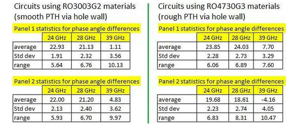
Fig. 6 compares the phase angle difference counts of microstrip channel transmission line circuits fabricated on different circuit boards at three critical 5G frequencies. The values on the left are the final results of the test for circuits with smooth metalized aperture wall exteriors, whereas the values on the right are the final results of the test for non-detailed metalized aperture wall exteriors.
As mentioned earlier, every effort was made to minimize the effects of material variations during the study, e.g., boards 1 and 2 were taken from the same large board to ensure that the difference in material Dk was minimized.
This is because the change in phase angle and whatever difference is revealed is mainly due to the effect of the circuit fabrication process. When analyzing the final results of circuits on the same board, the difference in phase angle from PCB processing and material variation is minimized because the same board is processed at the same time. Because of this, studying multiple circuits on the same board provides a good understanding of the quality of the metalized vias for the microstrip line circuits, and the PCB fabrication process may also result in a less delicate appearance of the metalized vias than expected. As shown in Figure 6, there is some variation in the phase angle of the S21 spread on each board, but this variation is not really significant when comparing the phase variation of the circuits on two different materials.
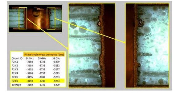
Fig. 7. Final results of the phase survey at three millimeter wave frequencies for the RO4730G3 material with exterior characteristic markings of the metallized perforated aperture walls (which are less delicate) from the top layer to the end layer of the circuit.
Obviously, after weathering the micrographs,the exterior walls of the metallized vias used to interface the top layer of circuitry with the bottom layer of circuitry may appear very different. For example, Fig. 2 shows the ID of P1/C1, which is a circuit metallized via made on 20 mil thick RO3003G2 material, and it has a very smooth metallized via wall. Figure 7 ID for P2/C6 circuit metallization perforation appearance, is in the thickness of 20.7 mil RO4730G3 circuit board material on the perforation,this material on the metallization of the perforation wall expression is a little more delicate.
From appearance alone,there might be some concern as to whether the RF performance would be affected by the finish of the metalized perforation walls.However,as the studies mentioned above have shown, the difference between non-fine and smooth metalized perforated sidewalls is only cosmetic,and there is absolutely no need to worry about their performance impact on RF/microwave/millimeter-wave performance,at least for these test circuits at 40 GHz.
It is important to understand that the information presented in this paper is only a small portion of the values brought together in the study of circuit materials with flat and smooth metallized vias and non-delicate metallized vias. The objective of the study was to demonstrate that the effect of the external finish of the metallized perforation walls on RF and millimeter-wave frequency performance is small.