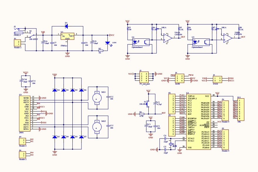
A schematic is a drawing representing the connection principle between the devices on the circuit board, printed circuit board schematics. PCB design, i.e. PCB Layout, is designed based on the schematic, through the analysis of the schematic and the other conditions of the circuit board constraints, the designer determines the location of the devices and the number of layers of the board, etc., the schematic lays out how the PCB will ultimately realize the connectivity, and constitutes a key part of the planning process. The schematic outlines how the PCB will ultimately achieve connectivity and forms a key part of the planning process.
Once the schematic is complete, the next step is PCB design. The design is the layout or physical representation of the PCB schematic, including the layout of the copper alignments and holes. The PCB design shows the location of the above components and how they are connected to the copper.
What should a perfect PCB schematic look like?
(1) Schematics in the electrical connections under the premise of the correct, drawings should try to achieve symmetry, uniformity, neatness, beautiful
(2) PCB layout should be reasonable and standardized, the alignment should not allow right angles, or sharp angles, and the same line width can not appear sudden changes, including power lines, ground lines, and signal line width settings should be reasonable.
(3) a variety of commonly used shortcuts to be mastered as soon as possible, to learn how to build and organize their library.
How do I see the PCB schematic, printed circuit board schematics?
(1) schematic symbols: need to understand the basic symbols of the components, such as capacitors, resistors, circuits, power supplies, and other basic symbols. In the PCB schematic, all components have fixed symbols and functions.
(2) Line symbols: Line symbols are wires that connect components, and different line symbols are used in PCB schematics to identify different connection relationships. For example, a solid line indicates a straight-line connection, while a dotted line indicates a connection line with an interval between two components.
(3) Design Layer: The design layer of the PCB schematic is the basic tool for PCB design, which includes the form design layer, signal layer, grouping layer, etc. The form design layer is used to define the PCB diagram. The shape design layer is used to define the shape and size of the PCB diagram, the signal layer is used to define the signal transmission path, and the grouping layer is used to define the layout of components.
(4) Design rules: In PCB schematic design, some design rules need to be followed. These design rules include component spacing, component layout, signal line length, and so on. These design rules help to maintain the stability and repeatability of the PCB diagram.

After the PCB schematic design is completed, PCB design needs to be started, and some basic design principles need to be followed when designing the PCB:
(1) input and output of the main circuit are clear and leave the laying of copper and punched holes in the location, pay attention to the placement of capacitors in the size of the principle;
(2) Download the chip datasheet, according to the recommended layout and wiring design;
(3) The layout of the switching power supply module should be compact, single line layout, as little as possible through the hole, pay attention to the placement of the key filter components should be reasonable;
(4) Input and output main circuit current-carrying processing: pay attention to the laying of copper current capacity and the number of holes;
(5) SENSE path: away from sources of interference and high current on the plane, do not directly connect the sense line in the switching power supply pins, generally use a 0.5mm line connected to the output filter capacitors after;
(6) The signal interconnection lines inside the switching power supply module all need to be thickened, generally thickened to more than 10mi1 (but not thicker than the pad);
(7) To ensure adequate heat dissipation, switching power supply cooling pads generally need to play the heat dissipation ground over the hole;
(8) Inductors and large capacitors are large and generally not placed on the welding surface and many other design points of attention.
In addition to the design principles mentioned above, designers also need to pay attention to the design phase to avoid many common problems, in order to follow up on mass production to pave the way for a good production base.
PCB schematic is the soul of PCB design, printed circuit board schematics, it not only provides a basic guide for PCB design but also ensures design accuracy, improves design efficiency, performance, and stability, and cost control plays an important role. Therefore, in the whole electronic design process, the schematic design and management must be highly valued. iPCB is a PCB manufacturer, providing PCB design and PCBA sampling services.