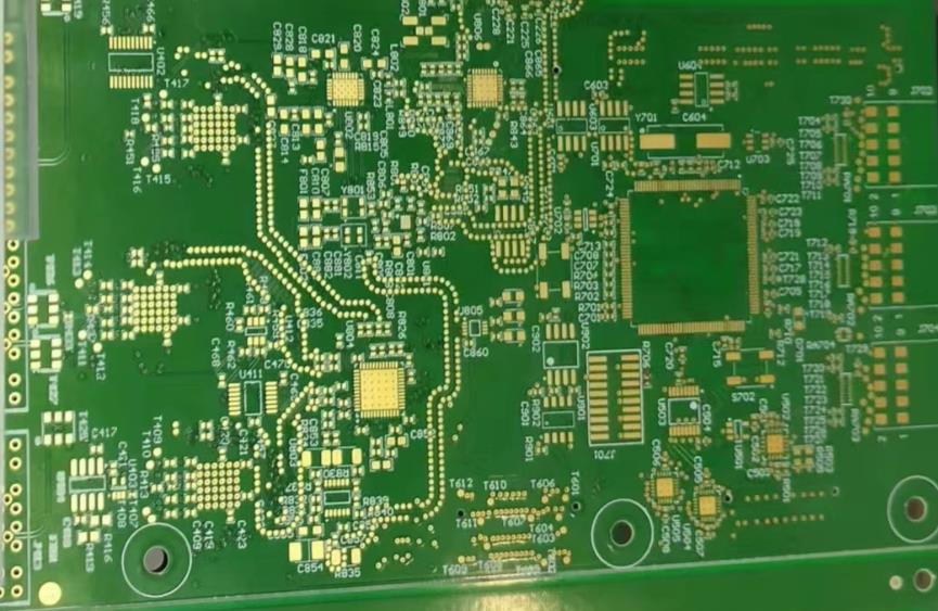
Several common standards for printed circuit boards
1) IPC-ESD-2020:Joint standard for the development of ESD control procedures.Includes the design, establishment, implementation and maintenance of the necessary ESD control procedures. Provides guidance for the handling and protection of ESD sensitive periods based on the historical experience of certain military and commercial organizations.
2) IPC-SA-61A:Post-solder semi-aqueous cleaning manual. Covers all aspects of hemi water cleaning including chemicals, production residues,equipment, techniques, process controls, and environmental and safety considerations.
3) IPC-AC-62A:Post-solder aqueous cleaning manual. Describes the cost of manufacturing residues, types and properties of aqueous cleaners,aqueous cleaning processes, equipment and technology, quality control, environmental control and employee safety, and cleanliness measurements and measurements.
4) IPC-DRM-40E: Desktop reference manual for through-hole solder joint evaluation.In addition to computer-generated 3D graphics,detailed descriptions of components, hole walls, and weld surface coverage are provided as required by the standard. Covers tin fill, contact angle, solder dip, vertical fill,pad coverage and numerous solder joint defects.
5) IPC-TA-722: Welding Technology Evaluation Handbook.Includes 45 articles on various aspects of soldering technology covering general soldering, soldering materials, manual soldering, batch soldering, wave soldering, reflow soldering, vapor phase soldering and infrared soldering.

printed circuit board
I.Automatic X-ray Inspection
Utilizing the difference of X-ray absorption rate of different substances,the parts to be inspected will be examined and defects will be found.It is mainly used to detect the defects of ultra-fine pitch and ultra-high density circuit boards, as well as the defects of bridging,missing pieces, and poor alignment produced during the assembly process. It can also be used to detect the internal defects of IC chips with its tomography technology. It is the only way to test the solder quality of the grating array and the blocked solder balls. The main advantage is the ability to detect BGA solder quality and embedded components without the cost of fixtures. The main disadvantages are slow speed, high failure rate, difficulty in detecting reworked solder joints, high cost, and long program development time. This is a relatively new test.
II.Laser inspection system
It is the latest development of PCB test technology. It uses a laser beam to scan the printed board, collect all the measurement data,and the actual measurement value and the preset qualification limits for comparison. The technology has been validated on bare boards and is being considered for assembly board testing. Fast enough for batch production lines. Fast output,no fixtures and visual unobstructed access are key benefits. High initial cost, maintenance and utilization issues are the major drawbacks.
III.Dimensional Inspection
The dimensions of holes, length, width and position are measured using a 2D image measuring instrument.Since the printed circuit board is a small,thin and flexible product, contact measurement can easily deform and lead to inaccurate measurement. Two-dimensional image measuring instruments have become the best high-precision dimensional measurement instruments.Sharp measurement of the image measuring instrument can be programmed to achieve fully automatic measurement, not only high measurement accuracy, but also greatly shorten the measurement time and improve the measurement efficiency.