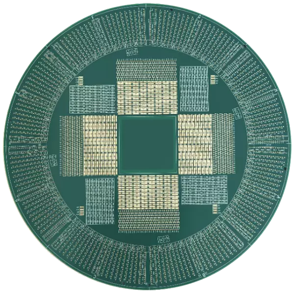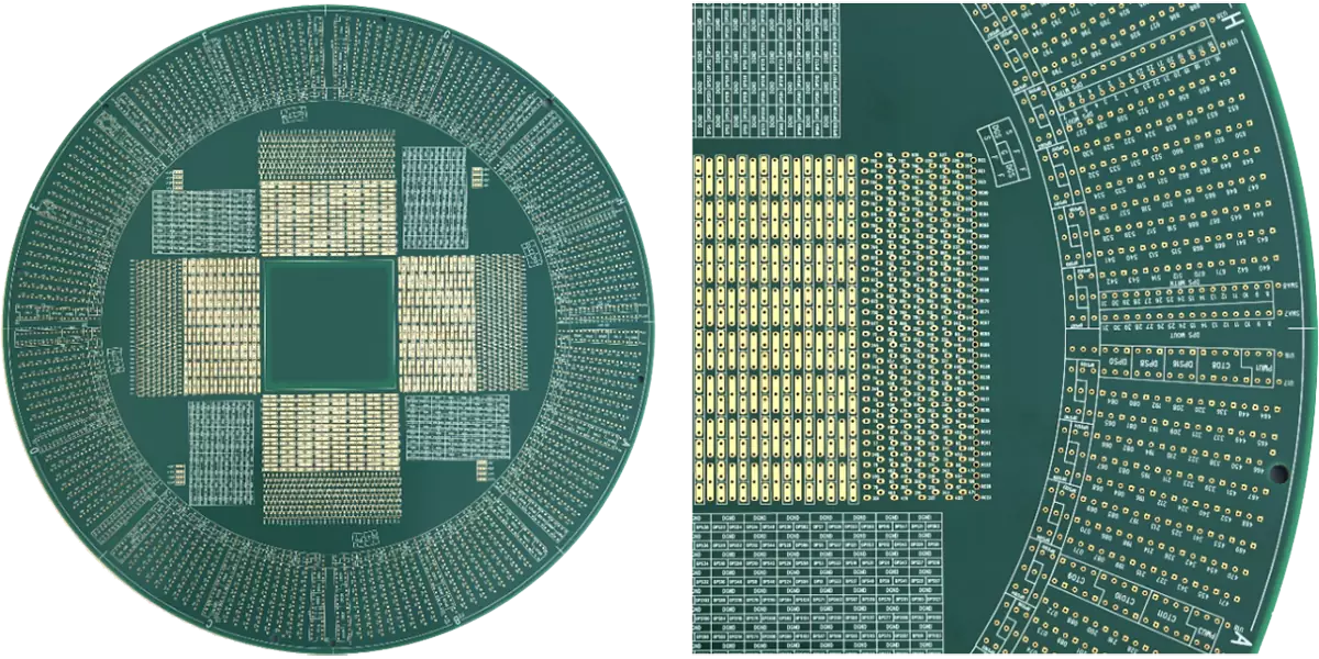
Product name: Probe card board
Base plate: VT901, 85N
Layer: 48L
Finished size: 20"*22"
Stacking: L1-L48 10mil
L1-L28 12mil
L29-L48 14mil
Surface treatment: Hard gold plating 3-15μ"
Special process: metal edging, fixed depth drilling
Product Application: Wafer Test Board
Probe card is a testing interface composed of probe pins, components, wires, and PCB. Depending on the situation, there may also be requirements for electronic components, stiffeners, etc., mainly for testing bare chips, i.e. wafer level testing.
Chip probing is an essential key joint in the semiconductor production process. Probe Card integrates tens of thousands of micrometer level probes onto a PCB board, and uses ATE and Prober to perform needle testing on each grain on the chip to determine its quality.
In recent years, semiconductor process technology has made rapid progress, ahead of the Moore's Law prediction rule for several years. Products emphasize lightweight and compact design, with IC volumes becoming smaller, functions becoming stronger, and the number of pins increasing. In order to reduce the area occupied by chip packaging and improve IC performance, Flip Chip packaging is widely used in graphics chips, chipsets, memory, and CPUs at present. The above-mentioned advanced packaging methods have a high unit price. If chip testing can be conducted before packaging and defective products are found in the wafer, they will be marked and discarded until the later packaging process, which can save unnecessary packaging costs.
The main purpose of a probe card is to directly contact the probes on the probe card with the solder pads or bumps on the chip, extract chip signals, and then cooperate with peripheral testing instruments and software control to achieve automated measurement. Probe cards are used for functional testing of bare crystal systems using probes before IC packaging, to screen for defective products and then proceed with subsequent packaging engineering. Therefore, Probe card is one of the important processes in IC manufacturing that has a significant impact on manufacturing costs.

Probe card PCB
Probe card type
1. U-Probe refers to a Probe card suitable for measuring storage devices. The probe area of U-Probe is equal to the wafer size, so the probe can be placed at any position on the wafer. The U-Probe used for DRAM has a crescent shaped DUT layout, which can make the most efficient use of space and fully utilize the resources of the tester.
The DUT layout reduces the number of contacts required for testing the wafer and achieves uniformity throughout the entire wafer to achieve optimal contact, thereby significantly improving the testing yield. Not only that, it also allows for wafer level detection using MEMS probe microcantilever and thin film multilayer technology.
2. Vertical Probe refers to a probe card suitable for multi chip testing of conventional logic products (including SoC and microcomputer products).
It is called a 'vertical' probe card because the probe needle is perpendicular to the substrate. Due to its short needle like structure and vertical contact with the device, the vertical type is most suitable for measuring small solder pads and high-frequency equipment.
3. MEMS-SP refers to a probe card used for logic devices, suitable for flip chip and fine pitch bump wafer testing of microprocessors and SoC devices.
Thanks to the vertical spring needle probe and MEMS technology manufacturing, MEMS-SP can perform high-precision and reliable testing with almost no variation. The structure of MEMS-SP allows for the replacement of single needles, thereby reducing maintenance time.
4. P-Probe refers to a vertical spring needle probe card. SP Probe for NAND flash memory is suitable for one touch testing of 12 inch wafers. Its high needle pressure specification helps achieve stable contact by contacting the gasket under the oxide film, and also allows for the replacement of a single needle for easy maintenance.
5. The probe card of wafer level chip level packaging (WLCSP) is suitable for testing array equipment in the testing area. The tip of the probe comes in crown and flat specifications, and you can choose one according to the testing environment.
As chip manufacturing processes become smaller and wafer foundry processes become more advanced, testing technology continues to improve. Probe card, as consumables in the testing phase, have increasingly high requirements for precision, yield, lifespan, and consistency.
Product name: Probe card board
Base plate: VT901, 85N
Layer: 48L
Finished size: 20"*22"
Stacking: L1-L48 10mil
L1-L28 12mil
L29-L48 14mil
Surface treatment: Hard gold plating 3-15μ"
Special process: metal edging, fixed depth drilling
Product Application: Wafer Test Board
iPCB Circuit provides support for PCB design, PCB technology, and PCBA assembly. You can request technical consultation or quotation for PCB and PCBA here, please contact email: sales@ipcb.com
We will respond very quickly.