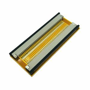
It is more cost-effective to conduct concept testing before entering the PCB manufacturing stage.A PCB prototyping board is a small device used to connect electronic components to ensure the smooth operation of the product.This process determines whether the proposed PCB design will be executed as expected,revealing any possible defects and enabling the designer to make necessary changes. At this stage, any other improvements or alternative solutions that the designer may have thought of were also introduced.The large-scale production of any new product cannot be separated from PCB prototyping services, which cannot be simply started without a prototype design phase.
The cyclic prototyping board,as a design that has been fine-tuned and validated for functionality and reliability, can accelerate the development of the final design. If a requirement or circuit board malfunction is discovered in the later stages of the process, the rework cost will significantly increase. This makes prototype design software a valuable tool for electronic engineers and circuit designers.

Prototypes are divided into several categories,and PCB designers may adopt a process of using multiple types of prototypes during the design and approval stages of a project:
Concept validation -This may include some expected functionalities aimed at proving the feasibility and reliability of circuit design concepts, but may not include all functionalities planned for this purpose—the final product.
Working prototype - includes all expected functionalities, but can be improved in the final design.
Visual Model - For illustrative purposes, adhere to the final physical design, but not the working prototype.
Functional Prototype - This stage should include all functions and features of the final production board. The possible difference is that manufacturing can be carried out on different devices, or even involve slightly different materials. This is usually due to different facilities provided to custom manufacturers. Some manufacturers may have separate areas where prototypes are developed based on rapid turns, rather than mass production lines that are more automated or use different manufacturing processes.
PCB prototyping board stage:
The first type is called breadboard testing or proof of principle, which will check whether the logic behind the PCB prototypiing board can be implemented. The next step is to check the expected size (preferred size) of the PCB prototype board. After this stage, a visual model is generated, and if approved, the final stage of functionality and appearance begins. The achievement, at this moment, is the closest approximation to the actual PCB prototype board. Usually, in PCB prototype design, the simulation of the current in the circuit board and the state of the circuit are the two most important processes. Actual components and materials can only be implemented for the final model or prototype before the simulation system works as required.
Perforated boards and performance boards are one of the available types of prototype boards. This category is also known as the "per-hole pad" design, where each hole has its conductor pad made of copper. With this setting, you can perform solder test connections between various solder pads. In addition, you can also wire between the pads on the perforated board. Stripboard, like other common prototype PCBs, also has separate hole settings for power strips. Instead of having only one conductor pad per perforation, copper bars extend parallel to the length of the circuit board to connect the holes, hence the name. These strips replace wires, and you can also disconnect them. Both types of PCB prototypes can be well used for planning boards. Due to the existing copper wire connection, the power strip can also be well used for planning simple circuits. Either way, you will use prototype board welding and prototype board wiring to test potential boards.
From breadboard to stripboard, if you have already completed any work on the prototype PCB, then you may have encountered a breadboard. These prototyping boards are very suitable for development and design, as you can move and modify components to establish plans. The breadboard can also be reused. In this regard, the component layout can be moved to the ribbon board for further testing. In addition, due to the ability to establish more complex connections, there are fewer restrictions on the prototype boards with strips and perforations. If the plan is to transfer from breadboards to peeling boards, it can help purchase peeling boards that match the direction or damage the traces of peeling boards. If you want temporary circuits to have a more robust and permanent configuration, moving the components from the bread to the stripping board is one of the most convenient methods.