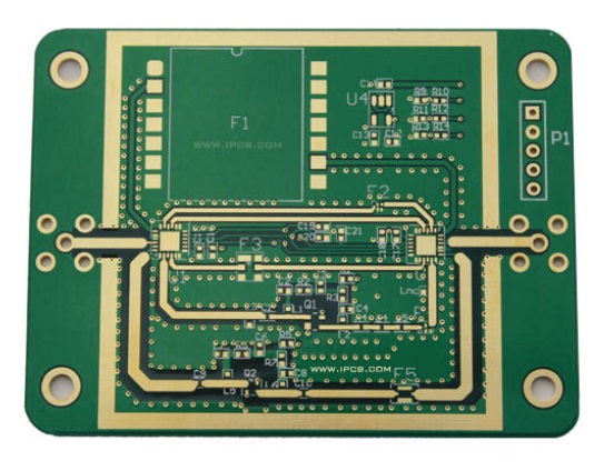
In high-frequency and high-speed PCB applications, PTFE (Polytetrafluoroethylene) is one of the most critical dielectric materials. Thanks to its ultra-low dielectric constant, extremely low dielectric loss, and excellent thermal stability, PTFE is widely used in 5G communication systems, millimeter-wave radar, satellite communication, aerospace electronics, and microwave RF modules. Among all its physical properties, the melting point of PTFE is one of the most important parameters, as it directly affects PCB manufacturing processes, thermal reliability, and long-term performance stability.
The standard melting point of PTFE is approximately 327°C.
This is significantly higher than conventional PCB materials. For comparison, the glass transition temperature (Tg) of standard FR4 epoxy resin systems is usually in the range of 130–180°C, and even high-Tg FR4 typically falls between 170–200°C. PTFE’s melting point is far above common PCB processing and operating temperatures, which is one of the main reasons it performs so well in harsh thermal environments.
It is important to note that PTFE is a crystalline polymer, so its “melting point” is different from the Tg concept used for FR4.
FR4 begins to soften once it exceeds Tg, causing a noticeable drop in mechanical strength and dimensional stability.
PTFE, however, remains solid and structurally stable until it reaches its crystalline melting point at 327°C. Below this temperature, its physical and electrical properties remain highly stable.
From real industrial data, PTFE typically starts to decompose chemically at temperatures above 500°C. This provides a very wide safety margin for PCB manufacturing processes such as lamination, soldering, and reflow.
A comparison of typical temperatures:
Process or Condition Temperature Range
Lead-free reflow soldering 245–260°C
PTFE melting point 327°C
PTFE decomposition temperature >500°C
Even at the peak temperature of lead-free reflow soldering (260°C), PTFE still has a safety margin of nearly 70°C below its melting point. This explains why PTFE-based PCBs can withstand multiple reflow cycles with minimal degradation in performance.
However, a high melting point does not mean PTFE is easy to process. On the contrary, PTFE is considered one of the most difficult PCB materials to manufacture. Its high thermal stability, strong molecular bonding, and extremely low surface energy create major challenges during fabrication.
First, lamination is significantly different from FR4.
FR4 relies on resin flow during pressing to bond layers together. PTFE has almost no natural flow behavior. Therefore, PTFE laminates are usually reinforced or modified, such as:
Glass fiber reinforced PTFE
Ceramic-filled PTFE
Modified PTFE composite materials
In multilayer PCB lamination, the pressing temperature is typically set at 350–380°C, higher than PTFE’s melting point, to allow the resin to melt, flow slightly, and then recrystallize to form a strong bond. This temperature is far above that of FR4 lamination (normally around 180–200°C), which means:
Special high-temperature presses are required
Temperature uniformity must be extremely well controlled
Tooling plates and release materials must withstand extreme heat

Second, drilling and hole quality are major challenges.
Near its melting point, PTFE exhibits high elasticity and ductility. During drilling, it is prone to:
Burr formation
Hole wall deformation
Resin smear
Therefore, PTFE drilling parameters are completely different from FR4. Typically:
Lower spindle speeds
Sharper drill bits
Strict post-drilling cleaning processes
are required to maintain hole quality and plating reliability.
Third, copper adhesion is a critical issue.
PTFE has an extremely low surface energy of only 18–20 mN/m, while FR4 usually has a surface energy of 40–50 mN/m. This means copper naturally does not want to adhere to PTFE surfaces. Without special surface treatments, plated copper can easily delaminate, leading to serious reliability risks.
To solve this problem, PTFE PCBs must undergo special processes before metallization, such as:
Chemical etching/roughening
Plasma treatment
Sodium-based surface activation (for certain PTFE systems)
These treatments increase surface roughness and chemical activity, allowing copper to bond properly.
From an electrical performance perspective, PTFE’s thermal stability is also directly linked to signal integrity. At high frequencies above 10 GHz, dielectric constant (Dk) and loss factor (Df) are sensitive to temperature fluctuations. PTFE maintains extremely stable electrical properties:
Dk variation within ±0.02 from –50°C to +200°C
Df variation typically within ±0.0002
This stability is crucial for radar systems, satellite communications, and high-speed digital designs where impedance consistency and low signal loss are mandatory.
Typical PTFE material properties:
Parameter Typical Value
Melting point 327°C
Decomposition temperature >500°C
Dielectric constant (10 GHz) 2.1–2.3
Dissipation factor Df (10 GHz) 0.0009–0.0015
Z-axis CTE 200–350 ppm/°C
Surface energy 18–20 mN/m
The Z-axis coefficient of thermal expansion (CTE) of PTFE is much higher than that of FR4 (FR4 is typically 60–80 ppm/°C). This explains why PTFE multilayer boards are more susceptible to via fatigue and copper barrel stress under thermal cycling. As a result, PTFE PCB design requires:
Larger annular rings
Optimized via structures
Thicker copper plating
Careful thermal management
In summary, the simple data point “PTFE melting point = 327°C” represents an entire high-end PCB manufacturing philosophy:
High melting point → exceptional thermal stability and suitability for high-frequency applications
High melting point → extremely demanding lamination processes and equipment
High melting point + low surface energy → complex metallization and adhesion challenges
High melting point → outstanding reliability during soldering and long-term high-temperature operation
This is why PTFE materials are much more expensive than FR4, yet remain irreplaceable in advanced communication, radar, and aerospace electronics. PTFE is not merely an “expensive material”; it is an engineering-grade material designed for extreme performance and extreme reliability.
If FR4 is the foundation of industrial PCBs, then PTFE is the “ceiling material” of high-frequency and high-speed PCB technology.