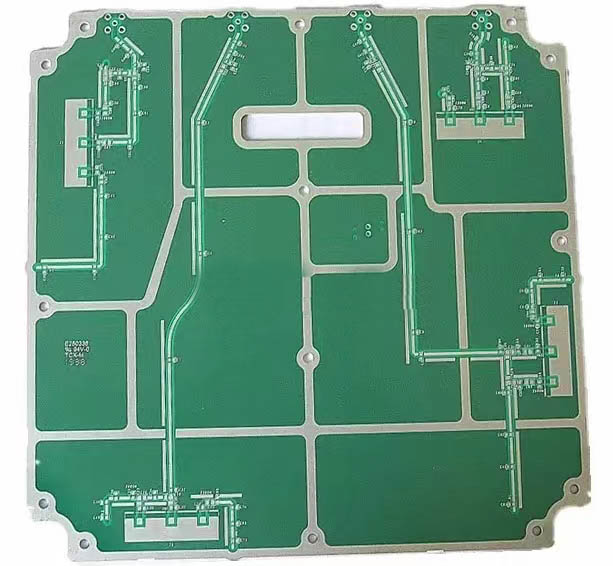
With the continuous development of communications technology, high confidentiality, high transmission quality requirements of mobile phones, car phones, wireless communications, to high-frequency development. The processing of high-frequency microwave PCB circuit boards also puts forward higher requirements. Here is IPCB to share with you the following basic requirements of high-frequency microwave PCB processing, to ensure that the processing of high-frequency microwave PCB circuit boards of high quality.
1.Dielectric constant, dielectric layer thickness, and copper foil thickness meet customer's drawing requirements.
Figuring out the dielectric constant, board thickness and copper thickness is a prerequisite for making high frequency microwave boards, because these factors have a great impact on product performance. In addition, the same substrate, at different frequencies, its Dk will also have a little change. From 500MHZ to 10GHZ, the dielectric constant of the plate changes by about 10%, PTFE changes in the smallest, the more for 0.5%.
2.Microwave PCB circuit board line width / spacing tolerance requirements are stringent
In view of the characteristics of high-frequency signal transmission, the requirements of microwave PCB circuit board characteristic impedance value is strict. Microwave PCB circuit board line width / spacing of the usual tolerance requirements are ± 0.02mm, more stringent ± 0.015mm.
Z0=8T/√(Dk+1.41)*ln5.98H/(0.8W+T)
Formula for calculating the characteristic impedance value Z0 of microstrip line structure.Where:Dk - dielectric constant,H - dielectric thickness,W - conductor width,T - conductor thickness.The control of the four parameters will effectively control the range of variation of the characteristic impedance Z0. Among these four parameters,the most influential is the dielectric thickness H,followed by the dielectric constant Dk,the lead width W,and the least is the lead thickness T. Once the data is selected, Dk is the most influential parameter.
Once the data is selected, Dk changes are small, H changes are small, T is easier to control, and the control of the wire width W becomes one of the difficulties in the production of microwave circuit boards after the completion of the engineering design of microwave PCB circuit boards.

Microwave PCB
3.Microwave circuit board wire quality control
This type of microwave PCB circuit transmission is not DC current,but high-speed electrical pulse signals. This is the fundamental difference with the traditional FR-4 microwave PCB circuit board. Because of this, pits, sawtooth, notches, pinholes, scratches and other defects on the lead wires are not allowed,such small defects will affect the signal transmission.
4.Polytetrafluoroethylene hole metallization difficulty
For polytetrafluoroethylene (PTFE) plate hole metallization processing,no matter double-sided or multi-layer boards, are required to thermal shock 288 ° C, 10 seconds, 1 ~ 3 times.
IPCB can provide fast and high-quality high-frequency microwave PCB processing service, please contact IPCB for more information.