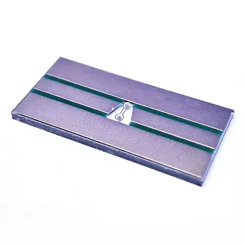
Substrate type: Sapphire
Substrate thickness: 0.5mm
Conductive layer: copper, nickel, gold
Metal layer thickness: 35μm
Surface treatment: Gold
Metal: 1L
Line width: 0.15mm
Application: Laser emitter
Sapphire Circuit Board is an electronic component assembly and connection technology that prints circuit patterns on sapphire substrates. Sapphire PCB circuit board have excellent physical and chemical properties, making them an ideal choice in certain specific application areas.
The composition of sapphire is alumina (Al2O3), which is formed by the covalent bonding of three oxygen atoms and two aluminum atoms. Its crystal structure is a hexagonal lattice structure. It is commonly used in cutting planes such as A-Plane, C-Plane, and R-Plane. Due to its wide optical transmission band, sapphire has good transparency from near ultraviolet light (190nm) to mid infrared light. Therefore, it is widely used in optical components, infrared devices, high-intensity laser lens materials, and mask materials.
Sapphire has the characteristics of high sound speed, high temperature resistance, corrosion resistance, high hardness, high transparency, and high melting point (2045 ℃). It is a material that is quite difficult to process, so it is often used as a material for optoelectronic components. At present, the quality of ultra-high brightness white/blue LED depends on the material quality of gallium nitride epitaxial (GaN), which is closely related to the surface processing quality of the sapphire substrate used. The lattice constant mismatch between the C surface of sapphire (single crystal Al2O3) and III-V and II-VI deposited films is small, and it meets the high temperature resistance requirements in GaN epitaxial process, making sapphire chips a key material for producing white/blue/green LED.
Characteristics of Sapphire Circuit Board
Physical properties: Sapphire substrate has extremely high hardness, second only to diamond, reaching a Mohs hardness level of 9. It also has high melting point, high thermal conductivity, and excellent optical transparency.
Electrical characteristics: Sapphire substrate has good insulation performance and high breakdown voltage, which can provide good electrical isolation and signal integrity.
Thermal stability: Sapphire substrate has a low coefficient of thermal expansion and excellent thermal conductivity, which enables it to maintain stability in high temperature environments and has good heat dissipation performance.
Corrosion resistance: Sapphire substrate has excellent corrosion resistance and high resistance to acids, alkalis, and chemical solutions.
Optical applications: Due to its high transparency and excellent optical properties, sapphire substrates are widely used in fields such as lasers, optoelectronic devices, and LED packaging.
High frequency electronic devices: Sapphire circuit board is widely used in radio frequency (RF) and microwave electronic devices due to their low dielectric loss and excellent high-frequency performance.
High power electronic devices: Sapphire circuit board can withstand high-power working environments and are suitable for the manufacturing of high-power electronic devices, such as power amplifiers and energy converters.
Optoelectronic devices: Sapphire circuit board have important applications in optoelectronic devices, such as Photodiode and Phototransistor.
Sapphire PCB substrate process
For sapphire substrates, they undergo several processes including cutting, rough grinding, fine grinding, and polishing before becoming a qualified substrate.
Cutting: Cutting is the process of cutting sapphire crystal rods into rough pieces with a thickness of around 500um using a wire cutting machine. In this process, diamond wire saw is the most important consumable.
Rough polishing: The surface of the sapphire after cutting is very rough and requires rough polishing to repair deeper scratches and improve overall flatness. This step mainly uses 50-80um B4C and Coolant for grinding, and the surface roughness Ra after grinding is about 1um.
Fine polishing: The next step is more precise processing, as it directly affects the yield and quality of the final product. The current standardized thickness of 2-inch sapphire substrate is 430um, so the total removal amount of precision polishing is about 30um. Considering the removal rate and the final surface roughness Ra, this step is mainly processed by Lapping with polycrystalline diamond liquid and resin tin disk.
Most sapphire substrate manufacturers use grinding machines to produce polycrystalline diamond liquid in order to pursue stability. For the micro powder of polycrystalline diamond liquid, it is generally required that the particle size be concentrated and the morphology be regular, which can provide long-lasting cutting force and relatively uniform surface scratches.
Sapphire Circuit Board has excellent physical, electrical, and chemical properties, making it suitable for electronic manufacturing in high-temperature, high-frequency, high-power, and optical applications.
Substrate type: Sapphire
Substrate thickness: 0.5mm
Conductive layer: copper, nickel, gold
Metal layer thickness: 35μm
Surface treatment: Gold
Metal: 1L
Line width: 0.15mm
Application: Laser emitter
iPCB Circuit provides support for PCB design, PCB technology, and PCBA assembly. You can request technical consultation or quotation for PCB and PCBA here, please contact email: sales@ipcb.com
We will respond very quickly.