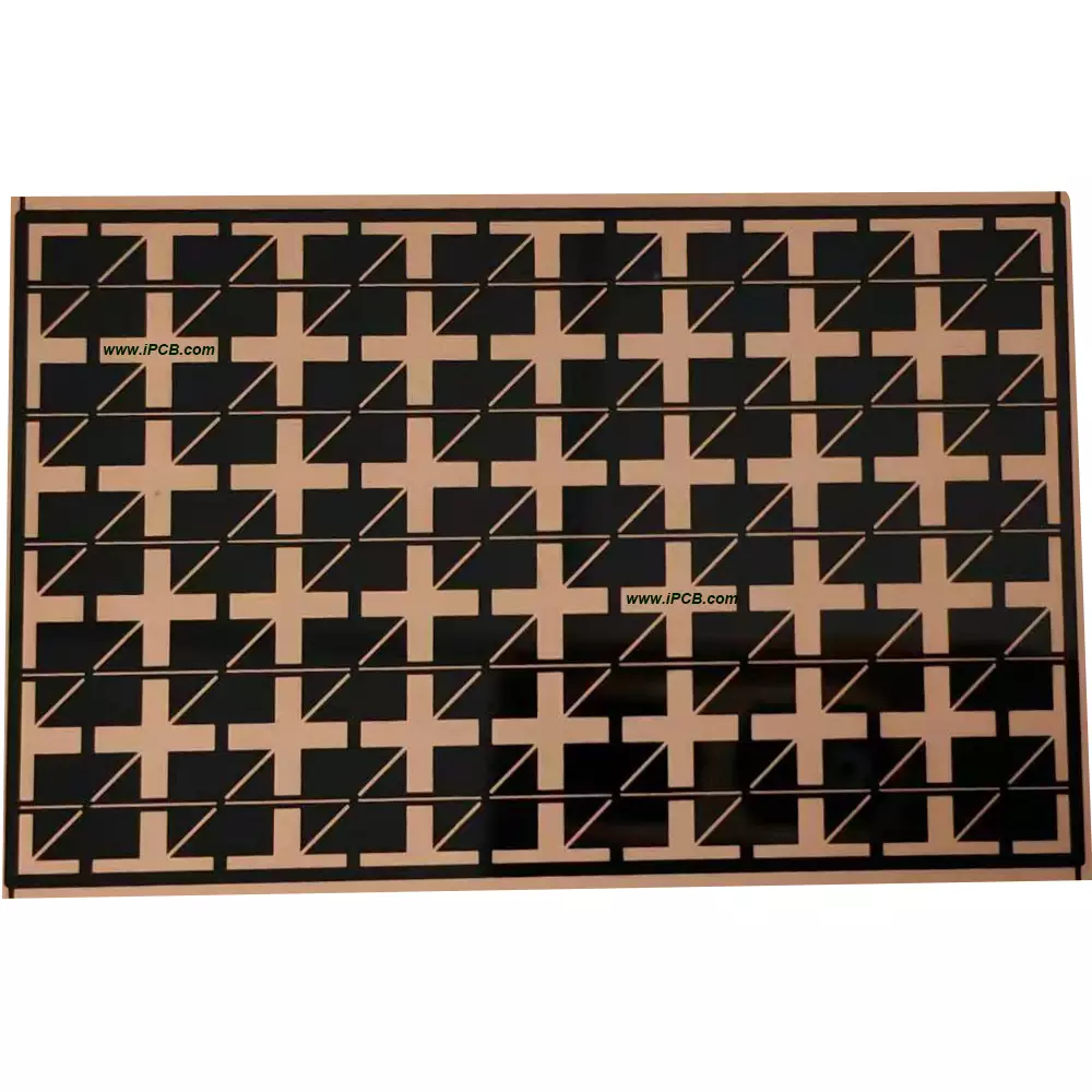
Substrate type: Silicon Carbide(SiC)
Substrate thickness: 0.1-2.0mm
Conductive layer: Copper, nickel, gold
Metal layer thickness: 35-400μm
Surface treatment: Gold
Metal: 1L
Line width: 0.25mm
Application: laser
SiC ceramic circuit board is renowned for their excellent thermal and electrical performance, as well as their ability to withstand high temperatures and harsh environments. They are used for high-temperature electronics and power electronics.
The new characteristics of SiC devices and the power density requirements for mobile applications pose new challenges to the packaging technology of power devices. The packaging technology of existing power devices is mainly developed on the basis of Insulated Gate Bipolar Transistor (IGBT) and Metal Oxide Semiconductor Field Effect Transistor (MOSFET), and has been evolving. However, these gradual improvements are not enough to fully utilize the performance of SiC devices, so the packaging technology needs revolutionary progress.
The essential characteristics of SiC devices determine their excellent indicators such as low internal resistance, high voltage resistance, high frequency, and high junction temperature. Under the pressure of continuously increasing power density in mobile applications, SiC devices have put forward new requirements and challenges for packaging technology.
The core of existing packaging technology can be summarized as soldering and bonding techniques, which I generally refer to as connection or bonding. For power modules, the connection directly related to the die/die is called the near end connection of the chip, while other connections are generally referred to as the far end connection of the chip. Regarding connections, most literature mixes them up as Attach, Contact, Connection or Join, Joining, etc. Some people also use Bonding to refer to all connections (combinations). Welding is used for die attach between the bottom of the chip and the substrate, or for system connection between the substrate and the heat dissipation substrate. The main welding methods include traditional SAC welding (SnAgCu Soldering), and in recent years, various brazing and diffusion welding have been developed. Bonding is used to connect the leads from the top of the chip to the substrate or from the substrate to the module frame. The materials commonly used are gold, silver, copper, and aluminum, with wire or strip shapes, and methods such as ultrasonic or hot pressing. In the past, the surface metallization material of power chips was usually Al or Al doped with a small amount of Si and Cu. The intermetallic compound formed by welding with the substrate surface (usually Cu) formed the die attach bonding layer. The metal on both sides of the substrate is often Cu, which is connected to the heat dissipation base plate through welding. The material of the heat dissipation base plate is usually aluminum SiC (AlSiC) or Cu coated with Ni on the surface.
The performance of these connecting devices could meet the requirements of most applications in early IGBT, but in recent years, they have increasingly fallen behind the development of semiconductor technology.
At present, the core process of power device packaging technology has shifted from aluminum based to copper based, and significant progress has been made in both preliminary research and practical product applications. In addition to bonding and welding connection types based on existing technologies, copper sintering has also made considerable progress. However, in terms of conductivity, thermal conductivity, shear force, melting point, and other indicators, these gradual improvements are not enough, so in recent years, the forefront research in the industry has mostly turned to silver sintering.
SiC ceramic circuit board
SiC material has a relatively high thermal conductivity and is an ideal choice for high-temperature circuit boards, such as automotive electronics, aerospace electronics, and other fields. In addition, SiC material also has advantages such as high temperature resistance and low energy consumption. However, the cost of SiC material is relatively high, and its hardness is also relatively high, making it difficult to process.
Even at 1400 ° C, SiC has good strength, extremely high thermal conductivity and resistance, good semiconductor conductivity, and high hardness.
SiC is the same as diamond, only with a different proportion of carbon. Therefore, SiC PCB has extremely high thermal resistance. For SiC PCB, working at 1000 ° C is easy. That's why they can be used in the field of lasers.
SiC has the characteristics of Si, therefore it has properties close to semiconductors. In other words, unlike other ceramic PCB, SiC PCB do not have high insulation properties.
At present, the manufacturing cost of SiC PCB is extremely expensive. But in the future, with the advancement of manufacturing technology, we can expect SiC PCB to have more applications.
Substrate type: Silicon Carbide(SiC)
Substrate thickness: 0.1-2.0mm
Conductive layer: Copper, nickel, gold
Metal layer thickness: 35-400μm
Surface treatment: Gold
Metal: 1L
Line width: 0.25mm
Application: laser
iPCB Circuit provides support for PCB design, PCB technology, and PCBA assembly. You can request technical consultation or quotation for PCB and PCBA here, please contact email: sales@ipcb.com
We will respond very quickly.