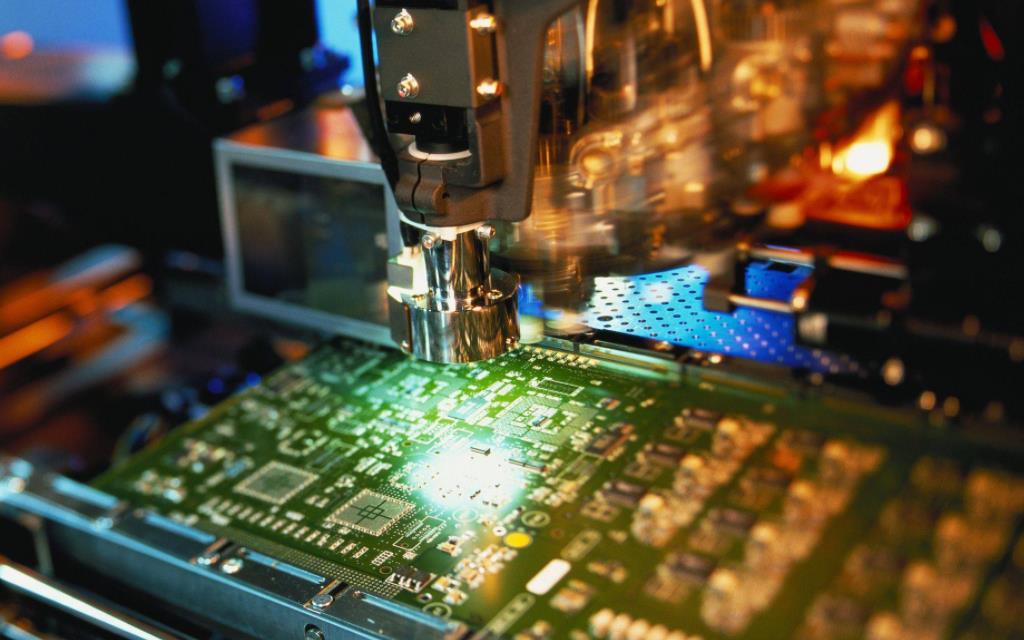
The manufacturing process of PCBA boards in electronic products uses surface mounting technology (SMT), which has replaced traditional through-hole insertion technology and dominated the development of electronic devices. It is widely recognized as a revolutionary change in electronic assembly technology. SMT aims to improve product reliability and performance, reduce costs, and bring about significant changes in both consumer electronics and cutting-edge military electronics.
Surface mount technology, also known as SMT. SMT is an electronic assembly technology that does not require drilling insertion holes on a printed circuit board, but directly solders surface assembled components to the designated positions on the printed circuit board, and uses solder to form mechanical and electrical connections between the components and the printed circuit board.
Electronic products that require SMT printing generally consist of printed circuit boards and surface mount components. Surface mount components include two categories: surface mount components and surface mount devices. Surface mount components refer to various passive components in the form of chips, such as resistors, capacitors, inductors, etc. Surface mount devices are electronic devices that use packaging, usually referring to various active devices, such as small outline packaging (SOP), ball grid array packaging (BGA), etc. Some components cannot be used for SMT, such as some connectors, transformers, large capacitors, etc

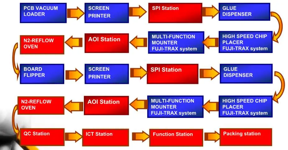
SMT process
SMT process
1. SMT includes two major processes: core and auxiliary.
The core process consists of three parts: printing, SMT, and reflow soldering, which are essential for the production of any type of product.
The auxiliary process mainly consists of a dispensing process and an optical-assisted automatic detection process, which is not necessary but is determined based on product characteristics and user needs.
2. The purpose of printing technology is to accurately print solder paste onto printed circuit boards through the combined action of templates and printing equipment.
The main process elements involved in printing technology include solder paste, templates, and printing systems.
Solder paste is important data for connecting and conducting components to printed circuit boards, achieving their electrical and mechanical connections. Solder paste is mainly composed of alloys and fluxes. During the welding process, they each exert their respective functions to complete the welding work.
Templates are used to accurately print solder paste onto printed circuit boards, and the production method and hole design of templates have a significant impact on printing quality.
The printing system mainly refers to printing equipment and printing parameters. The quality of printing equipment has a significant impact on printing accuracy. The reasonable matching of repeated printing accuracy and printing parameter settings of printing equipment is an important guarantee for accurate printing.
3. The purpose of the SMT mounting process is to ensure that all parts are accurately and quickly mounted onto printed circuit boards. The SMT process mainly involves SMT machines and their SMT capabilities.
The mounting capability of the mounting machine is an important guarantee for accurate mounting.
The key technologies of the SMT machine include high-speed motion, execution, and feeding mechanisms. Microtechnology. High-speed machine vision recognition and lighting technology. High-speed, high-precision intelligent control technology. Parallel processing real-time multitasking technology. Equipment open flexible modular technology and system integration technology.
4. Reflow soldering process is the mechanical and electrical connection between the soldering surface or pins of SMT components and the printed circuit board pads by melting the solder paste pre-allocated to the pads.
Reflow soldering ensures excellent welding results. The main process elements of the reflow soldering process are the reflow soldering furnace and its welding ability, which is mainly reflected in the heating system, cooling system, flux management system, and inert gas protection system of the reflow soldering furnace.
5. Auxiliary processes are used to assist in smooth installation and actively prevent testing and post-testing. The auxiliary process mainly consists of a dot-sticking process and an optical-assisted automatic detection process.
The dispensing process is to apply specialized adhesive to the bottom or periphery of the required components, providing appropriate protection to ensure that the components do not fall off after multiple reflow soldering cycles. Reduce the stress impact on components during installation. Protect components from damage in complex usage environments.
The process elements of the dispensing process mainly include dispensing equipment, specialized glue, and setting of dispensing parameters. Reasonable selection of equipment, glue, and well-designed parameter settings are necessary to ensure process effectiveness.
There are mainly two optical-assisted automatic detection processes.
1. Use specialized optical equipment to measure the uniformity of solder paste thickness and printing accuracy after printing. Check the accuracy of the patch after installation, detect defective circuit boards before reflow soldering, and issue an alarm promptly.
2. After reflow soldering, use specialized optical equipment to detect solder joints, detect circuit boards with solder joint defects, and issue an alarm. Specialized optical measurement equipment mainly includes visible light detection equipment and X-ray detection equipment.

SMT process flow
Single-sided SMT assembly
Incoming inspection ->Screen printing solder paste (dot patch adhesive) ->Patch ->Drying (curing) ->Reflow soldering ->Cleaning ->Testing ->Repair
Double-sided SMT assembly
A: Incoming inspection ->PCB A-side screen printing solder paste (dot patch adhesive) ->SMT ->drying (curing) ->A-side reflow soldering ->cleaning ->flipping ->PCB B-side screen printing solder paste (dot patch adhesive) ->SMT ->drying ->reflow soldering (preferably only for B-side ->cleaning ->testing ->repair)
This process is suitable for use when larger SMDs such as PLCC are mounted on both sides of the PCB.
B: Incoming inspection ->A-side screen printing solder paste (dot patch adhesive) of PCB ->SMT ->drying (curing) ->A-side reflow soldering ->cleaning ->flipping ->B-side dot patch adhesive of PCB ->SMT ->curing ->B-side wave soldering ->cleaning ->testing ->repair)
This process is suitable for reflow soldering on the A-side and wave soldering on the B-side of the PCB. In the SMD assembled on the B-side of a PCB, this process should be used when only the SOT or SOIC (28) pins are below.
Single-sided SMT mixed packaging process
Incoming inspection ->A-side screen printing solder paste of PCB (dot patch adhesive) ->SMT ->drying (curing) ->reflow soldering ->cleaning ->plugins ->wave soldering ->cleaning ->testing ->repair
Double-sided SMT mixed packaging process
A: Incoming inspection ->PCB B-side point SMT adhesive ->SMT ->Curing ->Flipping ->PCB A-side plug-in ->Wave soldering ->Cleaning ->Testing ->Repair
Attach first and insert later, suitable for situations where there are more SMD components than separate components
B: Incoming inspection ->PCB A-side plug-in (pin bending) ->Flipping ->PCB B-side point SMT adhesive ->SMT ->Curing ->Flipping ->Wave soldering ->Cleaning ->Testing ->Repair
Insert first and stick later, suitable for situations where there are more separated components than SMD components
C: Incoming inspection ->A-side screen printing solder paste of PCB ->SMT ->Drying ->Reflow soldering ->Plugs, pin bending ->Flipping ->B-side point SMT adhesive of PCB ->SMT ->Curing ->Flipping ->Wave soldering ->Cleaning ->Testing ->Repair
D: Incoming inspection ->PCB B-side point SMT adhesive ->SMT ->Curing ->Flipping ->PCB A-side screen solder paste ->SMT ->A-side reflow soldering ->Plugins ->B-side wave soldering ->Cleaning ->Testing ->Repair
A-side mixed installation, B-side adhesive installation. First, apply SMD on both sides, reflow soldering, then insert, wave soldering
E: Incoming inspection ->B-side screen printing solder paste of PCB (dot patch adhesive) ->SMT ->Drying (curing) ->Reflow soldering ->Flipping ->A-side screen printing solder paste of PCB ->SMT ->Drying ->Reflow soldering 1 (local soldering can be used) ->Plugin ->Wave soldering 2 (if there are few plug-in components, manual soldering can be used) ->Cleaning ->Testing ->Repair
The application of the SMT process in various fields of electronic products can directly affect the welding level of electronic product PCBA, as well as the performance and quality of the entire product.