SMT (Surface Mount Technology) assembly, also known as surface mount process, is currently the most popular technique in the electronics assembly industry. It offers advantages such as high precision, lightweight, and compact size, meeting the demands of modern miniaturized electronic products. To achieve high-precision placement and improve production efficiency, not only are higher standards required for the assembly process, but surface-mount components must also meet increasingly stringent criteria. So, what are the requirements of SMT assembly for surface-mount components? iPCB will provide a detailed explanation.
1. Component Layout Design
SMT assembly equipment is fully automated, high-precision, high-speed, and high-density. During soldering, both components and PCBs are subjected to reflow soldering. Therefore, strict requirements are imposed on component dimensions, dimensional accuracy, mechanical strength, heat resistance, and solderability. In summary, components must meet the criteria for placability, solderability, and soldering reliability.
(1) Component layout must be designed according to the characteristics and requirements of SMT assembly equipment and processes. Different processes, such as reflow soldering and wave soldering, have different layout requirements. For double-sided reflow soldering, the layouts for Side A and Side B also differ.
(2) Basic requirement for component layout in SMT processes: The distribution of components on the PCB should be as uniform as possible. Large or heavy components have higher thermal mass during reflow soldering, and excessive concentration may lead to localized low temperatures, resulting in cold solder joints. Additionally, uniform layout helps maintain balance, reducing the risk of component, plated through-hole (PTH), or pad damage during vibration and shock testing.
(3) Component orientation in reflow soldering: The placement direction of components should consider the PCB's movement direction in the reflow oven. To ensure simultaneous heating of both terminations of two-terminal chip components and both sides of SMD leads, tombstoning, misalignment, and pad lifting defects can be minimized.
(4) Clearance requirements: To prevent short circuits between conductive traces and the PCB edge during fabrication, inner and outer layer conductive patterns should maintain a minimum distance of 1.25mm from the PCB edge. Component spacing: The minimum placement spacing must meet the manufacturability, testability, and repairability requirements of SMT assembly.
2. Causes of Component Shifting
In SMT assembly, component shifting affects PCB functionality. Therefore, it is crucial to identify the causes and implement targeted solutions.
(1) Expired solder paste: Beyond its shelf life, the flux deteriorates, leading to poor soldering.
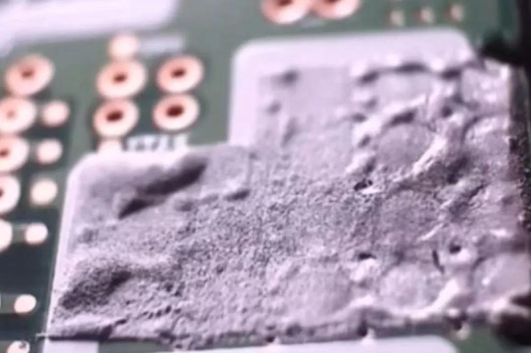
Component Displacement
(2) Insufficient tack force of solder paste: Components may shift due to vibration or improper handling during transport.
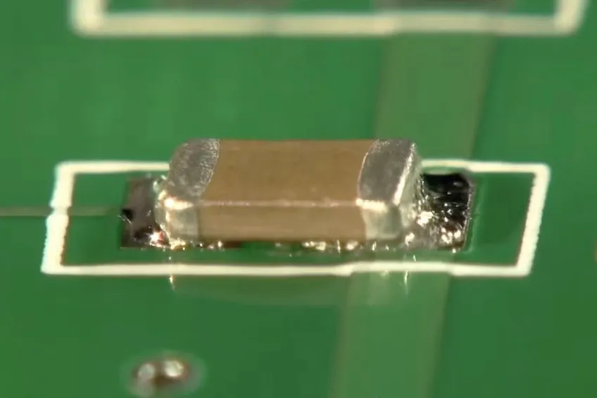
Not Sticky Enough
(3) Excessive flux content in solder paste: High flux flow during reflow soldering causes component movement.
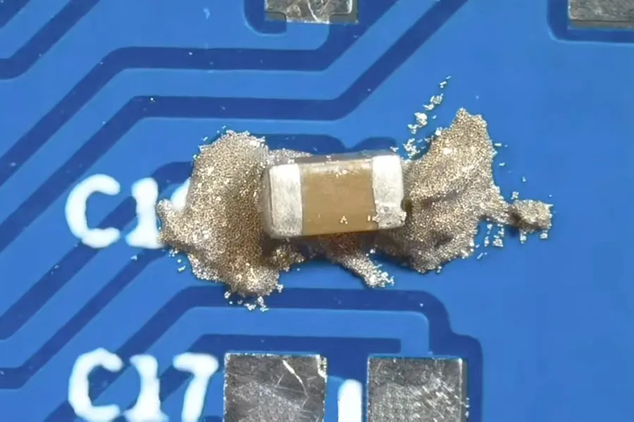
Flux Content
(4) Vibration or improper handling during PCB transport after printing or placement.
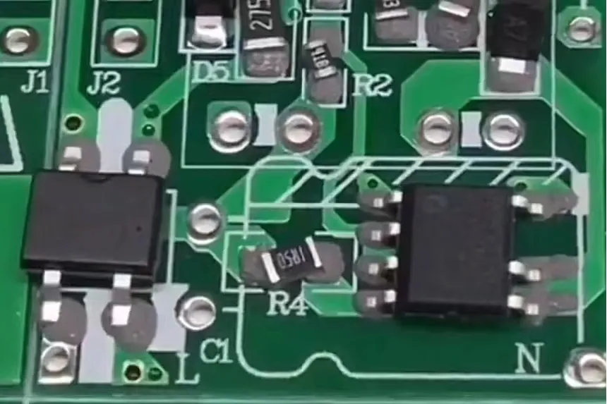
Transportation Method
(5) Incorrect nozzle pressure setting on the pick-and-place machine, resulting in insufficient force to secure components.
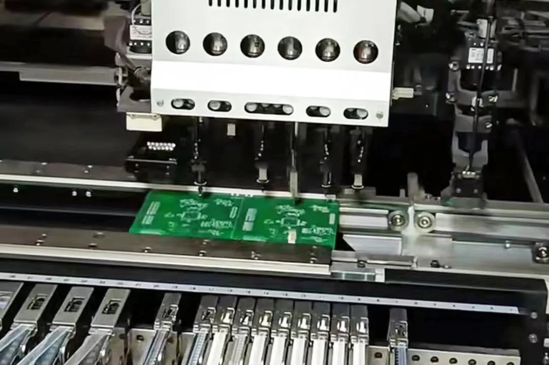
Nozzle Air Pressure
(6) Mechanical issues with the placement equipment, leading to misaligned component placement.
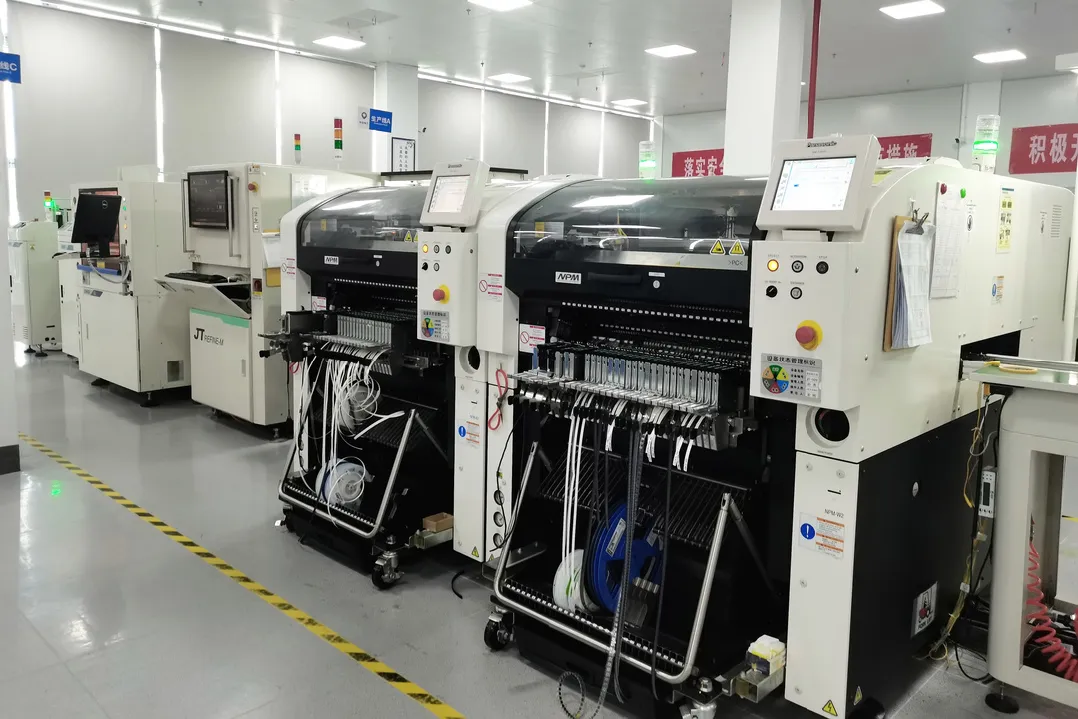
Mechanical Issues
3. Basic Requirements for Components
(1)Component shape must be compatible with pick-and-place machines, with surfaces suitable for vacuum nozzle pickup and flatness.
(2)Standardized packaging dimensions and shape, ensuring dimensional accuracy and consistency.
(3)Adequate mechanical strength to withstand placement pressure.
(4)Solderability of component leads must meet specifications:
(5)For leaded soldering: 235°C ±5°C, with ≥90% wettability.
(6)For lead-free soldering: 245–250°C.
(7)Heat resistance must meet lead-free reflow soldering requirements (260°C ±5°C).
(8)Compatibility with organic solvent cleaning processes.
(9)No deformed or oxidized component leads in packaging, which may affect placement efficiency.
Special Note: In lead-free SMT assembly, soldering temperatures can reach 260°C ±5°C for complex products. Therefore, component package heat resistance is critical. Different components have varying thermal endurance—some withstand thermal shock but not high temperatures, while others tolerate high temperatures but not mechanical stress. Thus, component parameters must be carefully reviewed during procurement.