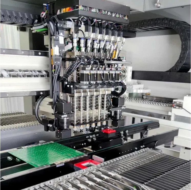
SMT PNP process is a technology that mounts electronic components directly onto the surface of printed circuit boards (PCBs) and welds them by means of reflow or wave soldering. With the increasing demand for miniaturization and efficiency,it has become a key technology in electronic manufacturing.
Compared with the traditional insertion technology, SMT has the advantages of high assembly density, small size, light weight, high reliability, and high production efficiency, so it is widely used in modern electronic equipment manufacturing.The smt pnp process offers unparalleled precision and productivity in producing advanced electronic products.
The role of PNP in SMT pnp process:
PNP helps to identify the polarity of electronic components, which is essential to ensure that components are correctly identified and placed during the placement process, avoiding boards that may not function properly due to incorrect polarity.
PNP polarity marking allows operators to identify components more quickly and accurately, thereby increasing productivity. Finally, accurate PNP marking helps to ensure the proper working performance of the board, ensuring a stable and reliable final product.
The application of SMT pnp process is mainly embodied in the key process of SMT placement, the process through the automatic placement machine will be mounted on the PCB according to the design requirements of electronic components. Operators need to place the components correctly according to the PNP polarity marking, and the PNP marking also plays an important role in other SMT processes such as reflow soldering to help arrange the soldering position of the components to ensure the quality and stability of the soldering process.
Basic Components:
Solder paste printing --> parts mounting --> over the furnace curing --> reflow soldering --> AOI optical inspection --> repair --> sub-panel --> grinding board --> washing board.
1.Solder Paste Printing:
Solder paste is printed onto the pads of the PCB board by stencil leakage,in preparation for the welding of components.The equipment used is the screen printing machine (printing machine), located at the forefront of this process production line.
2.Parts Mounting:
Electronic components SMD are accurately mounted to a fixed position on the PCB.The equipment used is the placement machine,located in the SMT production line behind the screen printing machine.Mounters are divided into high-speed machines and general-purpose machines:
High-speed machine: Used to mount components with small pin spacing.
General-purpose machine: Used for larger components with dense pin spacing.

High-speed machine
3.Over the Furnace Curing:
This step melts the patch adhesive, bonding the surface assembly components and PCB board firmly together. The curing furnace is used here and is positioned in the SMT production line after the mounter.
4.Reflow Soldering:
Through precise temperature and airflow control, the reflow soldering furnace melts the solder paste and wets the soldering ends of the components and PCB pads, forming a reliable welding connection. This step is critical in the smt pnp process, directly affecting the welding quality.
5.AOI Optical Inspection:
Auto Optical Inspection (AOI) checks the quality of solder joints and the placement of components on high-density circuit boards. However, AOI has optical limitations and may miss defects like solder joint issues under components.
6.Repair:
SMT rework involves removing defective, damaged, or misaligned components and replacing them with new ones. Visual inspections are conducted to check for missed, misaligned, or shorted components. If necessary, boards are sent to a professional rework station for repairs.
7.Sub-Board:
This step separates multi-connected PCBA boards into individual units, typically using V-cut or machine cutting.
8.Grinding Plate:
Grinding removes burrs from the PCB edges, making them smooth and flat.
9.Washing board:
After welding, the board is cleaned to remove rosin flux, tin balls, and other contaminants. This prevents short circuits and improves reliability. Cleaning involves placing the welded PCB in a cleaning machine to remove harmful residues and pollutants.
Advantages
High assembly density,small size,and light weight of electronic products.
High reliability and shock resistance,with a low solder joint defect rate.
Excellent high-frequency performance,reducing electromagnetic and radio-frequency interference.
Easy to automate, improving production efficiency and reducing costs by up to 30%–50%.
Saves materials, energy, equipment,labor,and time.
Thanks to the complexity and precision of the smt pnp process,there are numerous SMT PNP factories, especially in Shenzhen. With the rapid development of the electronics industry,this process services have become integral to modern manufacturing, driving innovation and growth in the industry.