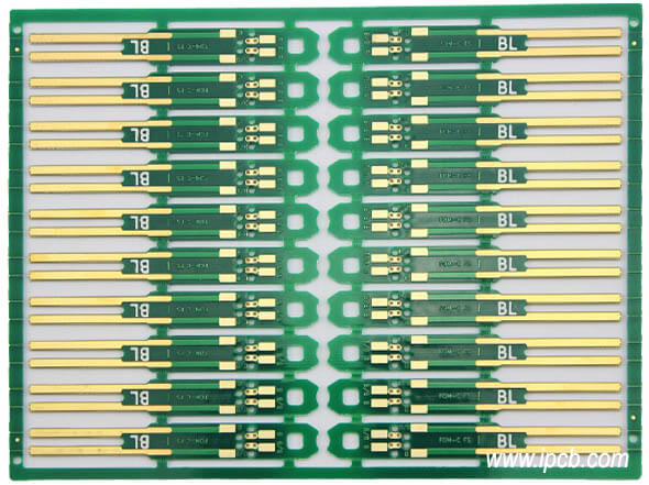
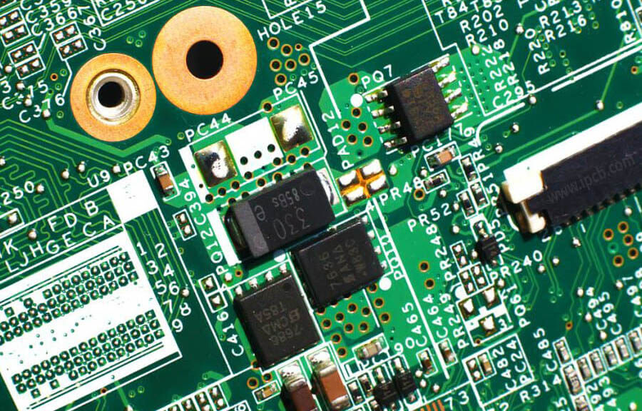
The basic principles of 3G, 4G, and 5G base stations are similar, but there are some differences in their specific designs. The 4G base station equipment mainly consists of three parts: baseband processing unit (BBU), remote radio frequency processing unit (RRU), and antenna system. At present, in 4G communication base stations, the antenna system and RU should use high-frequency PCB and high-speed PCB, while BU mainly uses high-speed PCB.
Baseband processing unit BBU: It completes functions such as channel encoding and decoding, baseband signal modulation and demodulation, protocol processing, and provides functions for upper layer network units.
RRU: It is the intermediate bridge between the antenna system and the baseband processing unit. When RRU receives signals, it uses filtering and low-noise amplification to convert them into optical signals, which are then converted into optical signals; When RRU sends to BBU, it converts the optical signal from BBU into an RF signal, amplifies it, and sends it through the antenna.
Antenna system: mainly used for signal reception and transmission, it is an information energy converter between base station equipment and end users.
From 4G to 5G, the attractiveness of base station structure and basic materials has not fundamentally changed, but there has been a significant improvement in dosage and parameters. Therefore, the research on the structure of 4G base stations and the application of high-frequency PCB have certain reference significance for 5G.
The antenna, as a device for energy conversion, directional radiation, and reception, is the core of the entire base station operation. It mainly consists of five core components (4G base station antenna): radiating unit, feeder network, reflector, packaging platform, and antenna controller (RCU).

High frequency PCB
Calculation of PCB consumption for 4G base stations
The PCB used are mainly divided into antenna system RRU and BBU. Based on a BBU pulling three pairs of antennas and three pairs of RRUs, the total area of the antenna system PCB is approximately 0.684 square meters, and the total area of the antenna system PCB is approximately 0.3 meters. The total area is 0.984 square meters.
According to industry research information, the average price of 4G antennas and RRU PCB is around 2500 yuan/square meter. As for the RRU and antenna components of a single base station, the ASP is around 2500 yuan. BBU section, size approximately 440X86X310mm
The number of BBU boards is between 3-6, and each board is connected to the backplane through an interface. The distribution of slots and configuration principles for BBU boards in BBU are as follows: GTMU occupies 5 and 6 channels as the main control transmission unit, while other plug-in boards can install TDL boards and main control boards. The boards can achieve interface functions, and the received CPRI data can be forwarded to other boards.
The total area of the main control board, star card board, baseband processing board, and baseband RF interface board is about 0.3 square meters, the power board is about 0.03 square meters, the surge board is about 0.008 square meters, and the total value per station is about 992 yuan.
For CCL, in 4G base stations, the high-frequency PCB CCL required for antennas and amplifiers is less than 5G. Generally, hydrocarbon or polytetrafluoroethylene materials are used, mostly pressed together with ordinary FR4. High speed PCB copper-clad laminates are mainly used in other fields such as BBU, and their materials can be modified with FR4. Generally speaking, high-frequency and high-speed copper-clad laminates account for about 20% of the value of base station PCB, equivalent to a global market space of approximately 102 billion yuan per year.

5G PCB
The pace of technological change and evolution brought by 5G
As of January 2019, GSA has 201 operators in 83 countries, including 5G commercial testing, pre commercial, and commercial operations. Especially in regions such as the United States, South Korea, Japan, the United Kingdom, and China, they are the earliest countries to carry out 5G commercial construction, and will achieve 5G commercial network construction in 2019-2020.
China's three major telecom operators have conducted 5G commercial testing in five major cities. China Mobile plans to install 1000 5G base stations in 2019 and conduct commercial testing nationwide in 2020.
Technologically, other manufacturers actively participate in the research and development of 5G baseband chips and terminals, promoting the maturity of the 5G industry chain.
In terms of chips, Qualcomm and Samsung released commercial 5G chips at the end of 2018, and MediaTek will also launch its own 5G baseband chips in 2019.
The maturity period of mobile terminals is relatively long. The 5G mobile phone and independent baseband chip based on 7-10 nanometer process are expected to be launched in 2099. The 5G mobile phone based on SOC multi-mode chip platform is expected to be commercially available in the second half of 2020. In the future, with the development of terminals, products such as small wearable 5G terminals and full band 5G smartphones that use the latest RF front-end technology are expected to mature in 2021.
The PCB value of 5G macro base station is about 15104 yuan/station, the PCB values of indoor substations are about 30% and 40% macro stations, and the PCB value of 5G macro base station is about 5286 yuan/station. The PCB value of 5G macro base station is 3.2 times that of 4G (4692 yuan), and there is still greater room for improvement.
Considering the progress of 5G construction, assuming the layout rhythm of macro base stations and indoor substations from 2018 to 2022, the construction of 5G base stations can bring incremental market space for PCB within one year (assuming that the value of single station PCB&CCL decreases by 6% annually).
It can be seen that at the peak of 2022/2023, the demand for PCB brought by the construction of 5G base stations in a single year is about 210 billion yuan to 24 billion yuan (of which the Chinese Mainland accounts for about 50% -60%), almost three times the demand of 8 billion yuan in the 4G era.
The communication PCB market is generally dispersed, but the demand and pattern for high-end rails are good. The global communication market size is about 12 billion US dollars, with the top five accounting for only about 20%, but in reality, the main participants in PCB (or high-frequency materials) with 18 or more layers are the first tier. In the process of upgrading storage devices caused by communication substitution and data flow explosion, when the trend shifts upwards to PCB links, the increase in value and usage is often based on high-level quantities, new materials, and new process PCB products However, low-level PCB (mainly used for some secondary links or low-end devices) are not as flexible in terms of demand changes as high-level PCB, and primary manufacturers are the main ones benefiting from value and consumption growth. There are moats in technical barriers, fixed assets investment barriers, commercial barriers, certification time difference barriers and so on.